4bit ADC DAC Schematic
| First Download Schematics and Symbols from the directory for simulation of ADC connected to DAC building in LTSpice. The file were download and LTSpice simulation was started. Run the program, The Picture fig1 show the real and ideal circuits behaviour same as in LTSpice. 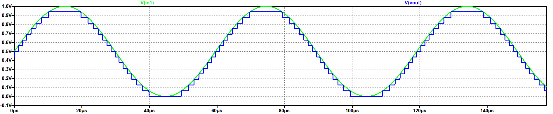
|
| In FFT changed number of data point samples in time. Then selected both Input and Output.. In picture fig2 show input signal better than output signal because of 4bit and it was noisy. |
| We used again 4Bit_ADC_DAC_Pipe for Ramp test. That is why we need another voltage source with the help of pulse input. Pulse voltage source V1 is connected to in 1 and sine voltage sourceV2 is disabled. 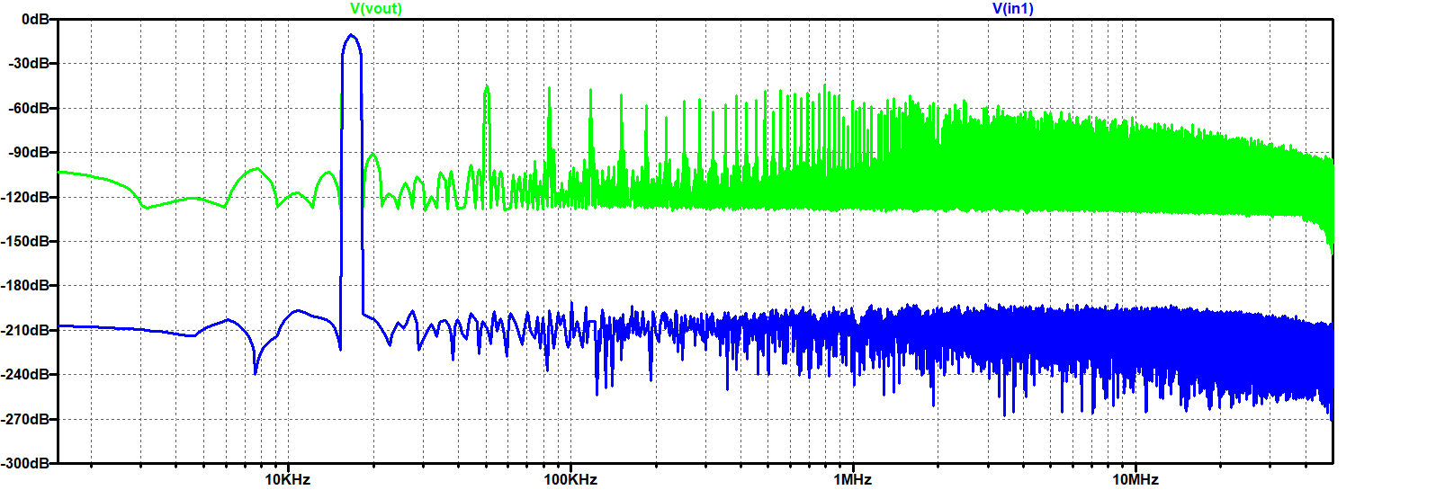
|
4Bit ADC DAC Ramp Test
| We used again 4Bit_ADC_DAC_Pipe for Ramp test. That is why we need another voltage source with the help of pulse input. Pulse voltage source V1 is connected in 1 and sine voltage sourceV2 deactivated. In picture shows 4Bit ADC DAC Ramp analysis 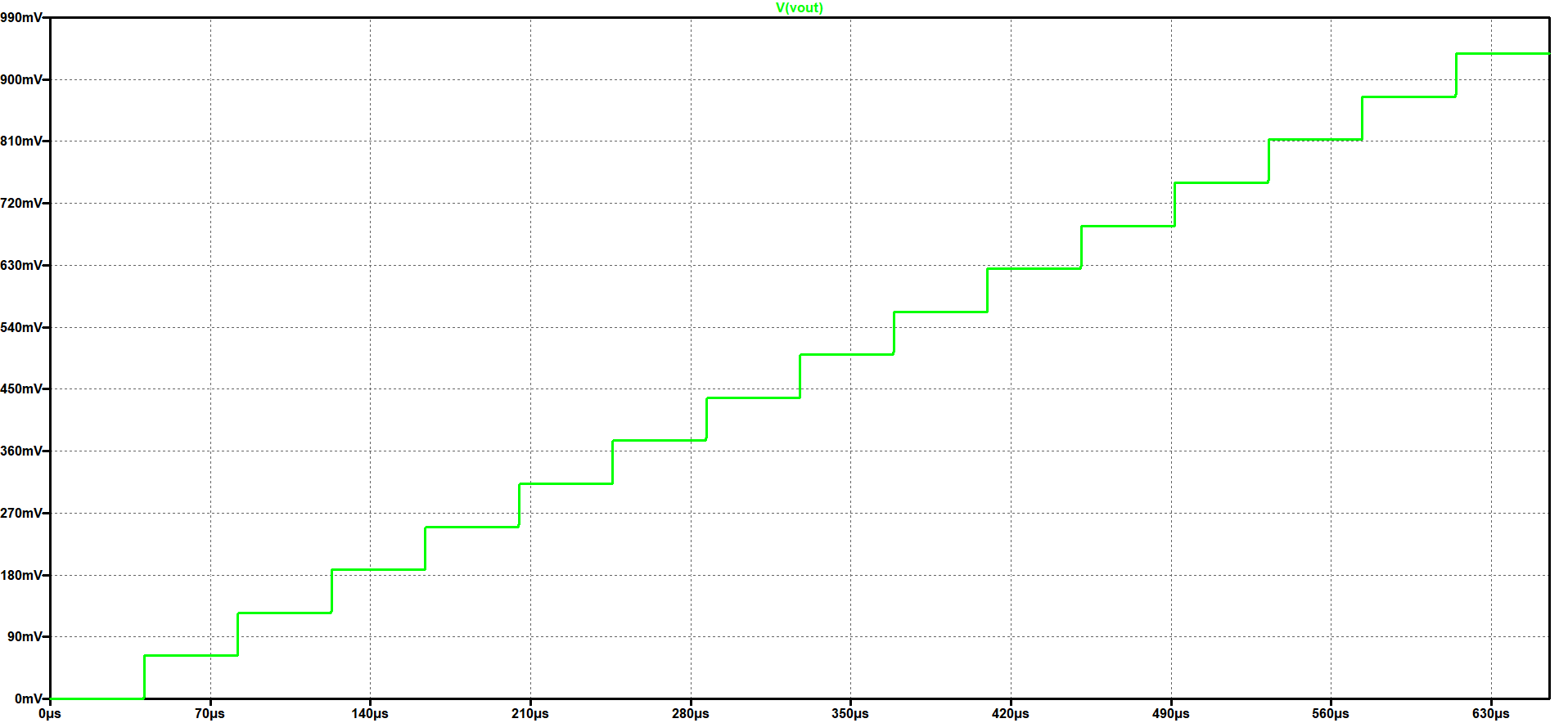
|
4bit ADC DAC INL,DNL,with a Ramp Analysis
| Now, we run again the 4Bit ADC DAC test simulation in LTSpice with a ramp . Then in the LTSpice Extract the simulated values with Read Raw File. In the Read LTSpice raw data site shows 1.Extracted values 2.Map values to integer 3.DAC INL,DNL analysis 4.ADC Histogaram In picture shows 4Bit ADC DAC Ramp analysis 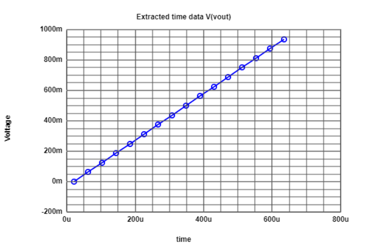 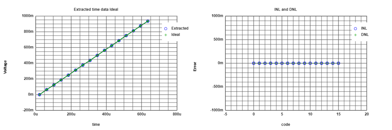
|
4Bit ADC DAC Ideal Histogram Test
| We used again 4Bit_ADC_DAC_Pipe for Ideal Histogram test. Changed Time step for Histogram ramp test. In Pictures shows many code and many outputs. In picture shows diffrent step size in histogram test 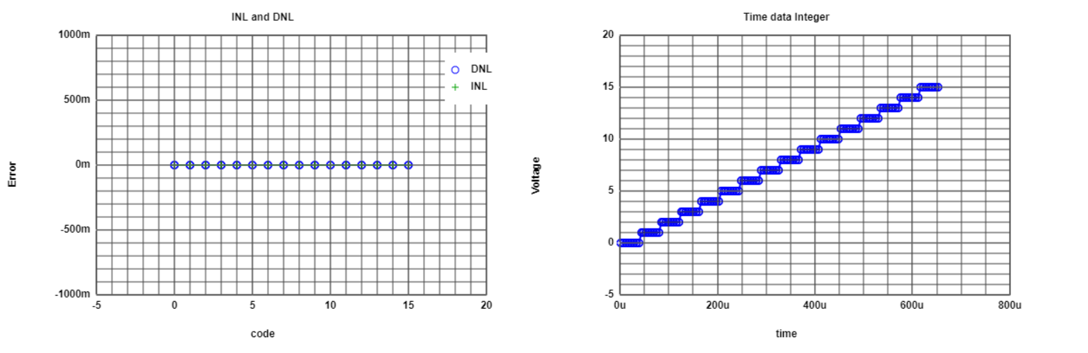
|
4Bit ADC DAC Sine Test
| In the LTSpice, disabled pulse voltage source V1. Run the data file we got sine curve shows in pictures. 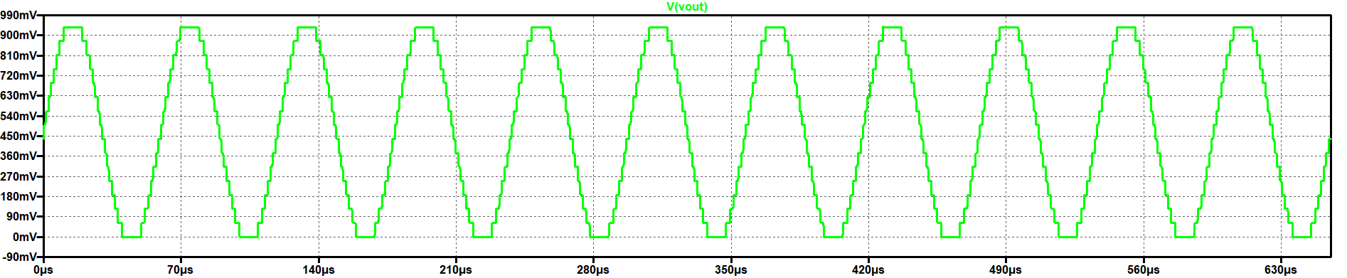
|
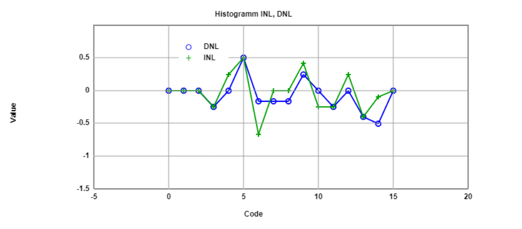
4bit ADC DAC INL,DNL,with a Sine Analysis
| We again open the Read Raw Data file and put the value Stop time and Time step. Run the data file we got sine Extracted value curve, shows in pictures. We was able to see ADC histogram test curve. Pictures shows in the graph error value is not Real but values is in Average 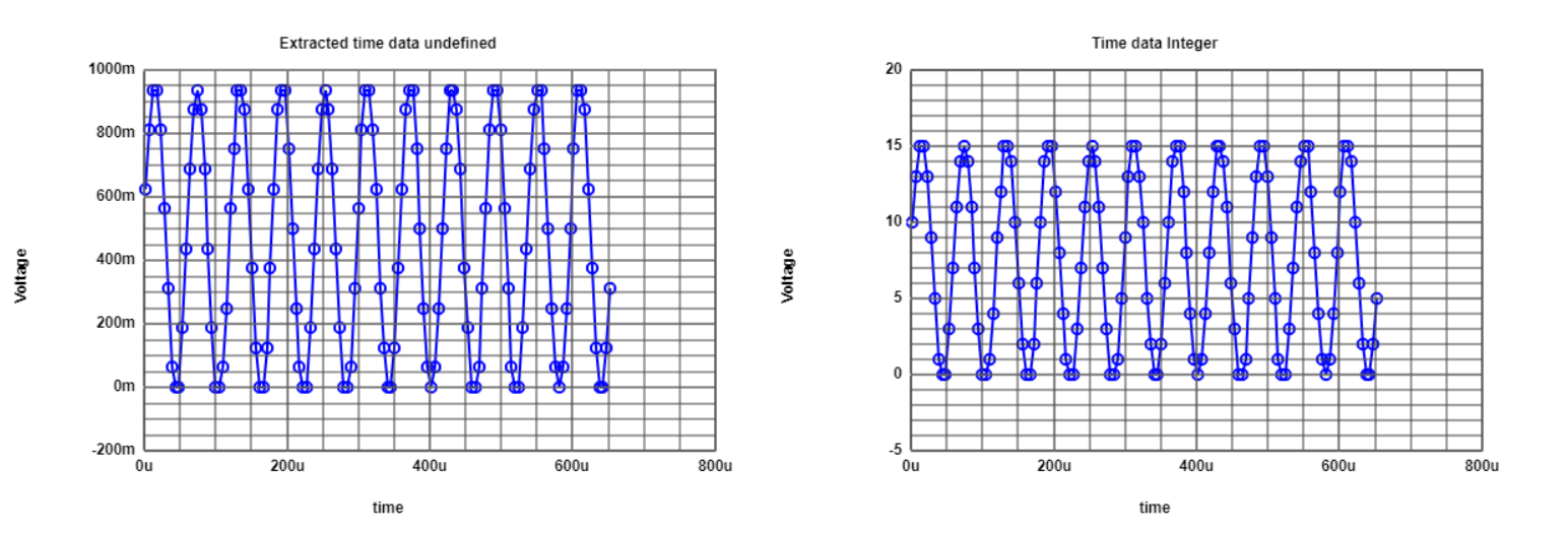 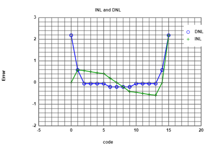
|
4bit ADC DAC FFT with a Sine Analysis in Javascript
| So, First We go to the Map to integer. We got values, select and copy then, we was go to the FFT data processing in new link, it was javascript file. Then put the input data in input code then read the positive integer data. Got the 128 Numbers of points, then Genarated diffrent FFT charts, shows in pictures. In the 16Bit INL DNL Curve values was missed the code so we had to change the number of bits 10 to 4. we are able to see real INL DNL sine, ramp signal outputs in FFT analysis. 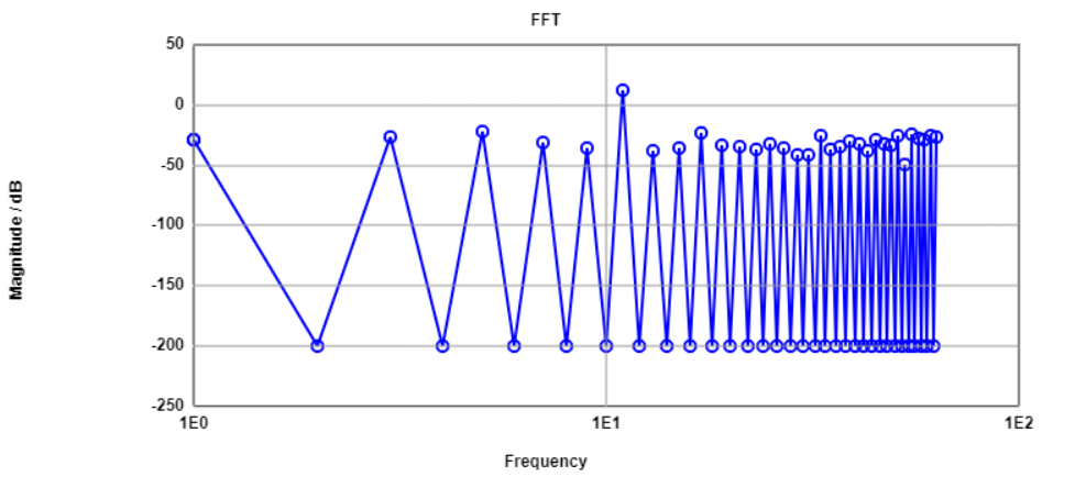 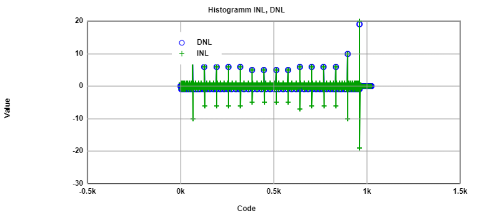
|
Simulation R2R DAC Converter with a sine signal
| 4Bit DAC converter was replaced with 4Bit R2R DAC converter in LTSpice The Ramp and Sine input signals were same. open R2R DAC then copy the circuit R2R and paste in the 4Bit DAC ADC. Then sine signal was given as the Input FFT analysis was done to observe the INL and DNL parameters. Then output of 4Bit DAC ADC converter disabaled. Then run the data and analysed the R2R converter Vout. Now, some filled error in R2R converter so, modify the values of resistors in R9 1.5k and in R6 1.3k. Then the Run the program, The pictures shows Big jump in the center beacuse we added some errors. 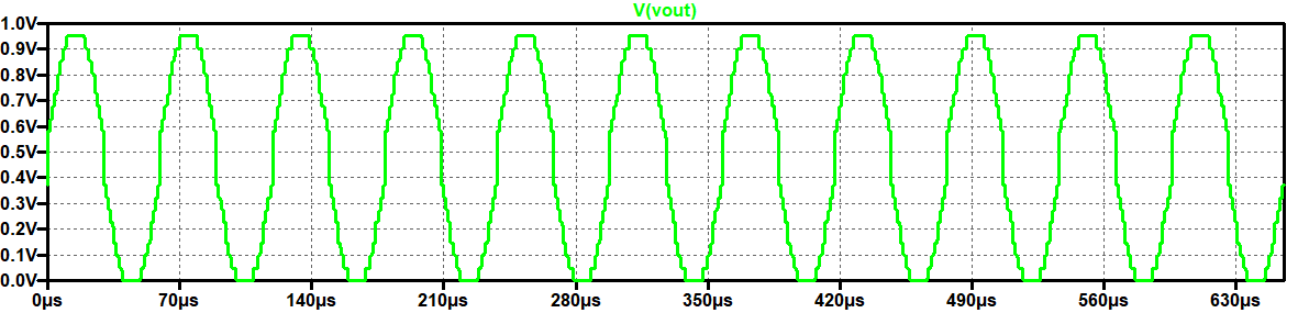 After added error After added error |
4bit R2R INL, DNL, FFT a sine signal Analysis
| Then, again went to Read Raw Data file, put the values of Stop time and Time step. Then, analysed the Map to integer and extracted values for R2R Converter. Then copied the integer data values and put in the FFT data Processing in input code. Got the 128 Numbers of points, then Genarated diffrent FFT charts, shows in pictures. We saw and analysed INL and DNL of Histogram. pictures show R2R INL DNL sine signal outputs in FFT analysis.  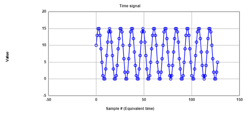
|
4bit R2R signal to Noise Analysis
| In the Table we show the values of frequency and Magnitude. with the some frequency increases,However signal magnitude decreases. 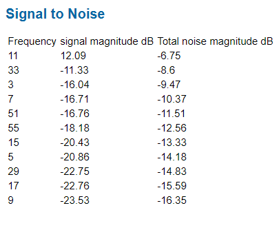
|
Simulation R2R DAC Converter with a ramp signal
| Again. changed the voltage source from Sine to Pulse signal voltage input. Then, analysed the Ramp signal of R2R Converter. In picture shows Ramp signal jump in the middle high pulse. 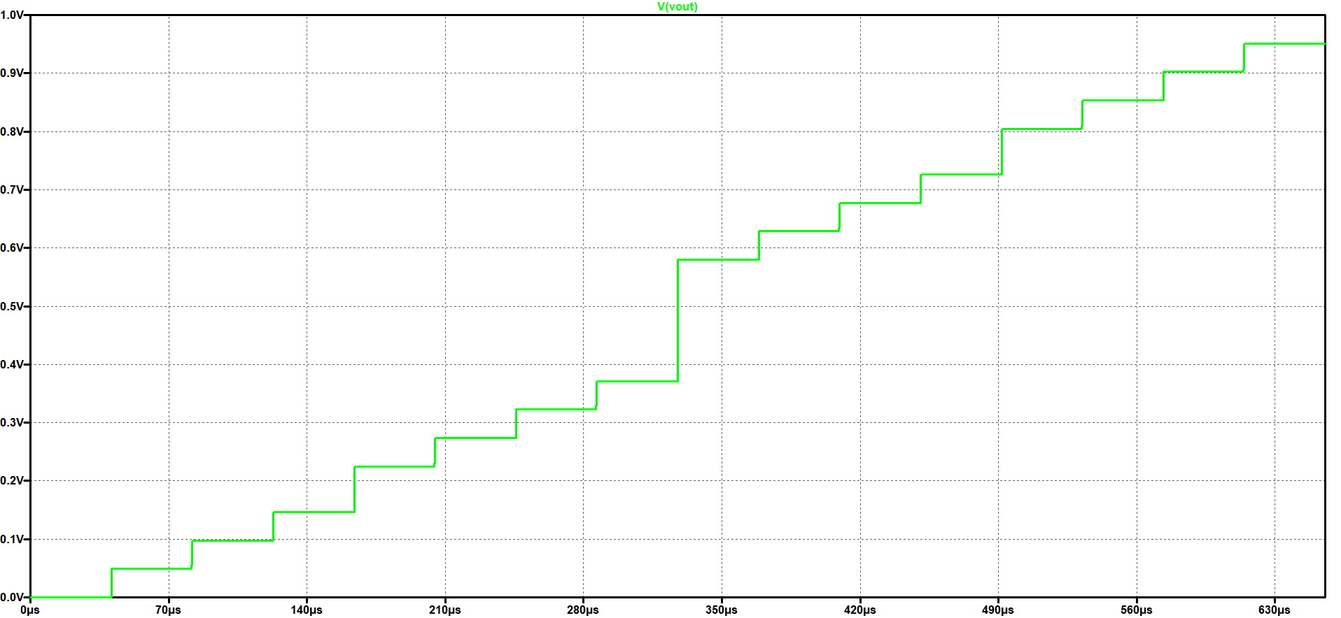
|
R2R INL,DNL,with a Ramp Analysis
| We again open the Read Raw Data file and put the value Stop time and Time step. Run the data file we got ramp Extracted value curve, shows in pictures. We was able to see ADC histogram test curve. Pictures shows in the graph Real ADC values. 1. graph shows Extracted data value. 2. graph shows Time data integer value. 3. graph shows Ideal Extracted Time data value. 4. graph shows INL and DNL error value.  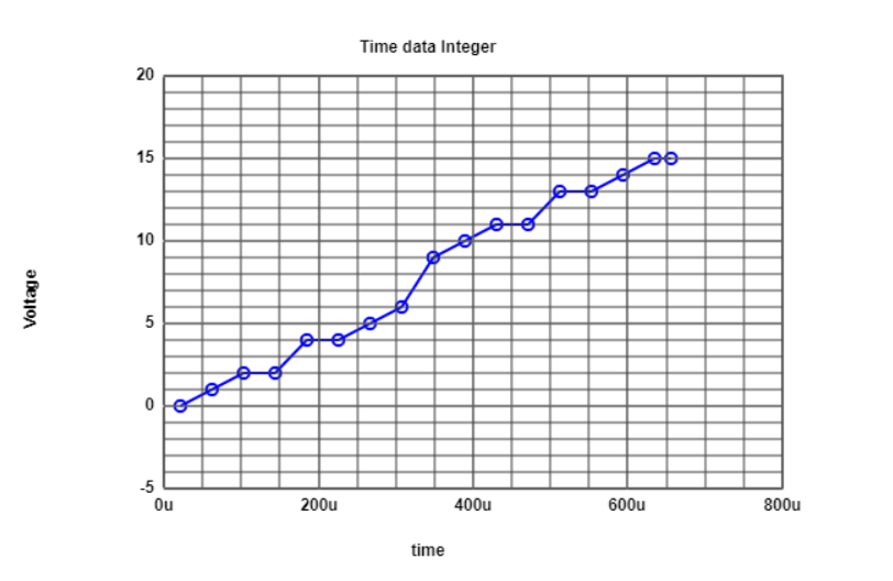 
|
Conclusion
|
We have observed the behaviour of 4 bit ADC and DAC converter when a ramp and sine signal are input. In optimum or ideal conditions
INL and DNL values were observed to be zero and can be deduced that there were no error in conversion. Once the DAC parameters were
changed, it was observed that the INL and DNL values obtained beyond +1 and -1 which can be concluded due to the non optimisation of
the DAC parameters.
|