ADC DAC Schematic and Simulation Graph
|
The schematic shows a 4-bit ADC DAC simulation set up. Simulate a ramp test. 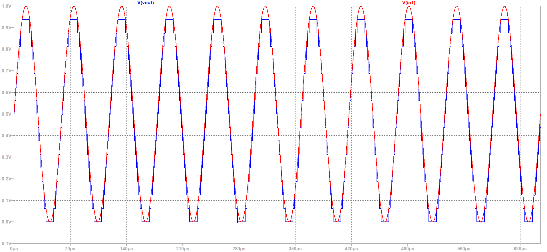 We have input voltage V2 which is a SINE signal containing 0.5V offset, 0.5V amplitude and 16784.66796875 Hz frequency. There is also a clock signal for ADC and DAC with 10ns sample rate. Input Voltage: V2 in1 0 SINE(0.5 0.5 16784.66796875) FFT of 4bit ADC and DAC: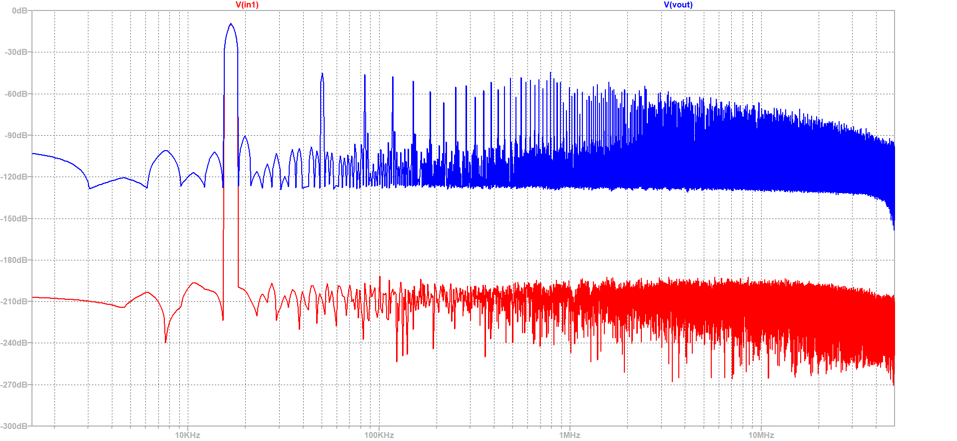 From the FFT Simulation it is visible that our output signal has more noise than input signal. |
Ramp Test
|
If we want to use a circuit for a ramp we need a voltage source. The voltage source V1 connected between in1 and ground. The Ramp Voltage source V1 is given below: V1 in1 0 PULSE(0 1 0 655.36u 655.36u 0 1310.72u)After doing simulation of the Ramp signal I got the below graph. 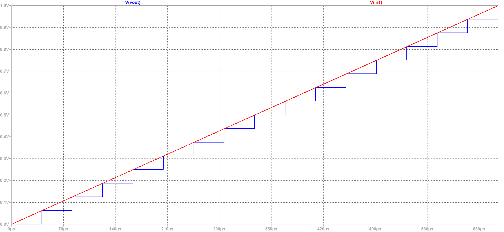 From this graph it is observable that there are 16 steps in this curve and the step size is fixed. Now for data analysis we need to do filtering. By using a java script tool we can do this. In this case I went to Read Raw File to extract our LTSpice data so thst we can do this filtering. This java script can read a LTSpice RAW file and filter the output with a certain time step. To do this filtering I selected below datum: Start Time: 0 Stop Time : 655.36E-6 Time Step : 40.96E-6There are 16 steps on the graph and our simulation time is 655.36E-6. So the time step is 40.96E-6. After loading the Raw file I got the following results: Expected Values: 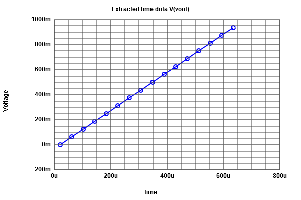 DAC INL,DNL Analysis:  For ADC Histogram test we need more time steps and in this case I used 5.12E-6s. Now reload the Raw file again. ADC Histogram test:  For SINE Signal: First we need to disable the ramp signal and active the SINE Signal in order to analyse the Histogram test for ADC. Then again reload the Raw file to extract the data.  Now after taking the values (input values) from sg table we can do FFT analysis for the SINE signal. FFT Analysis:  The above signal is 10 bit. After calculating the SNR (range) I found 4 bit signal. Here is the Graph: 
Simulation R2R DAC
4-bit R2R Modified DAC:
In this Circuit I modified resistence (R) values: R6=1.3k, R9=1.5k and  4Bit_R2R_DAC_FFT_Simulation_graphs: Voltage Source: V2 in1 0 SINE(0.5 0.5 16784.66796875)  From this simulation it is observable that there are errors in the signal especially at the pick and at the bottom of the INL and DNL signals. Now Active the Ramp Signal to do the FFT Simulation again. Voltage Source: V1 in1 0 PULSE(0 1 0 655.36u 655.36u 0 1310.72u)  Ramp Signal Raw Data Analysis for R2R DAC: name: 4Bit_ADC_DAC_pipe.raw UTF16: 1 type: size: 39971692 bytes No. Variables: 2 Extracted Variable: V(vout) No. Points: 3330877 header: Title: * C:\Users\Moniruzzaman Likhon\Desktop\Interface Electronics\web_Template\InEl_P2019\2020_GroupC2_V3_Likhon\LTSPICE\4Bit_ADC_DAC_pipe.asc Date: Sat Nov 07 01:57:59 2020 Plotname: Transient Analysis Flags: real forward nocompression No. Variables: 2 No. Points: 3330877 Offset: 0.0000000000000000e+000 Command: Linear Technology Corporation LTspice XVII Backannotation: x4 clk in1 vdd d0 d1 d2 d3 out Backannotation: x1 clk d0 d1 d2 d3 in1 vdd out Backannotation: x4:x1 p1 p2 clk vdd Backannotation: x1:x1 p1 p2 clk vdd Variables: 0 time time 1 V(vout) voltage  Ramp Signal FFT Analysis for R2R DAC:  Measurement Instruction: Code: 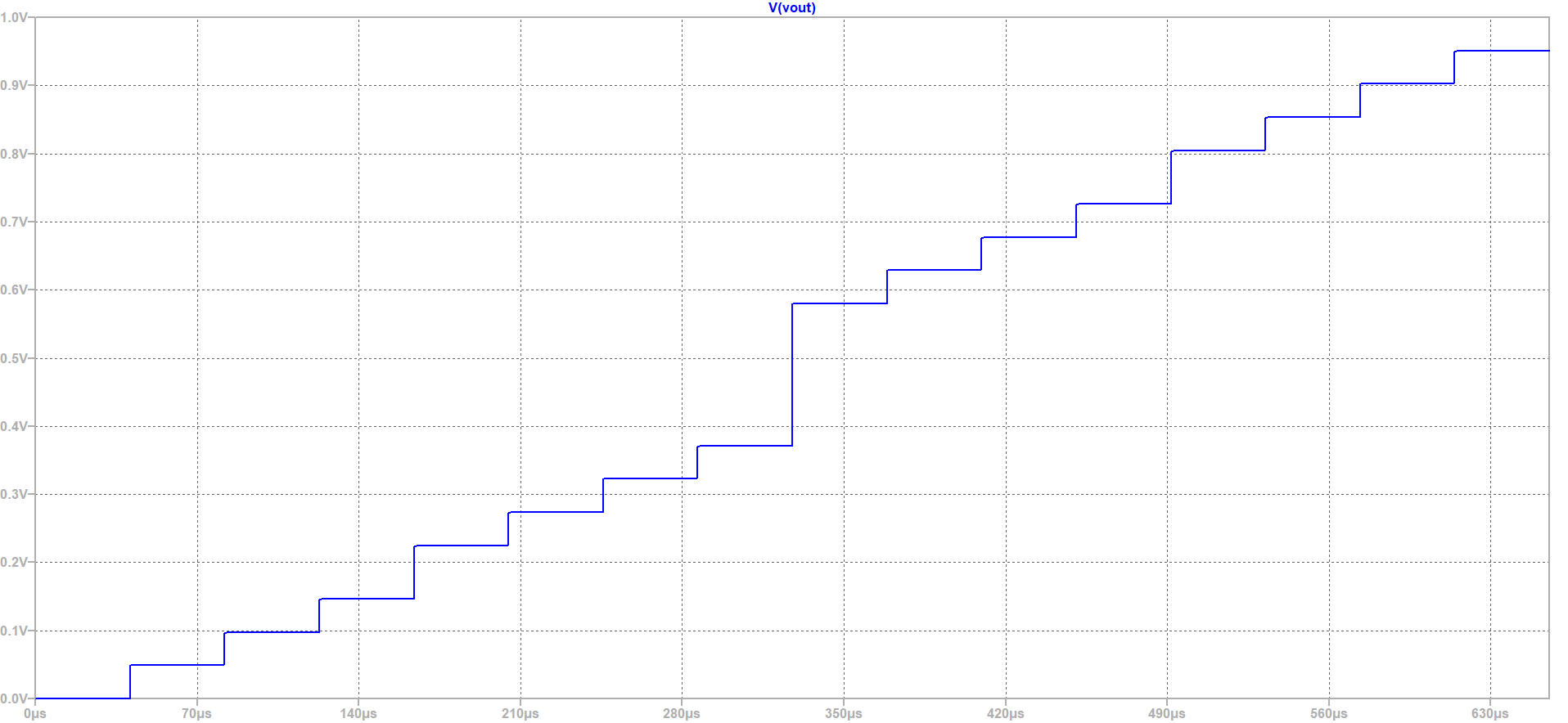 |