Interface ElectronicsLaboratory 01Group C03, ****59, M |
Overview
- Install webpage template
- Download LTSPICE files
- Simulation analysis
- Summary
Installation of webpage
- Download the template.zip file
- Unzip the file
- Goto Directory InEl_P2019
- Copied Directory 2019_GroupX to 2020_Group<xx>_<Lastname>
- In the directory copy the file: 2017_Group01_V00.html to 2020_Group<xx>_V1_<Lastname>
- Edit with Notepad++ or other text editor: 2020_Group<xx>_V1_<Lastname>
- Change the header, change the footer, made slide overview, installation
Test for 4 Bit ADC and DAC
|
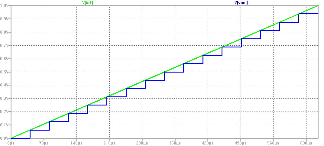
A 4 Bit ADC and DAC test can be simulated in LTSPICE. The files were downloaded and LTSPICE simulation was started. The output file size is limited by using the .save dialog option. A voltage source was added with a ramp from 0 V to 1 V with a rise time of 655 µs.br> The picture shows a ramp input voltage and the DAC ramp output voltage over 16 steps can be seen. With a measurement statement the voltage levels were measured. .Measure TRAN V0000 FIND V(Vout) AT=20u At 60 us time the output 0f 0.0625 V ist given for the code 0001. V0001: V(Vout)=0.0625 at 6e-005 No error in the voltage level can be seen. It is an ideal ADC and DAC.  |
Test for a 3 Bit DAC
|
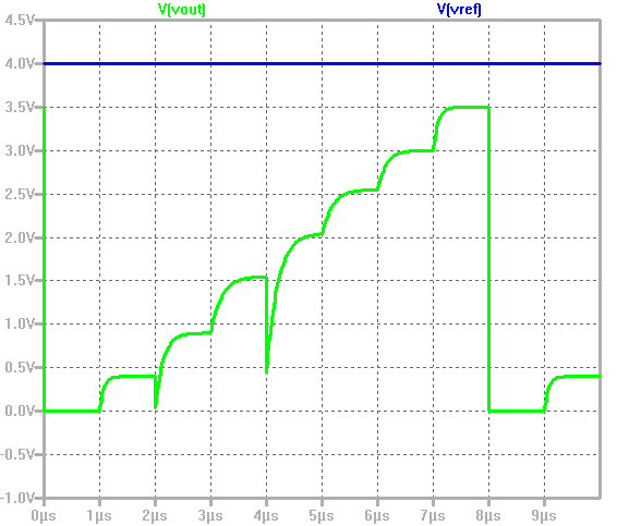
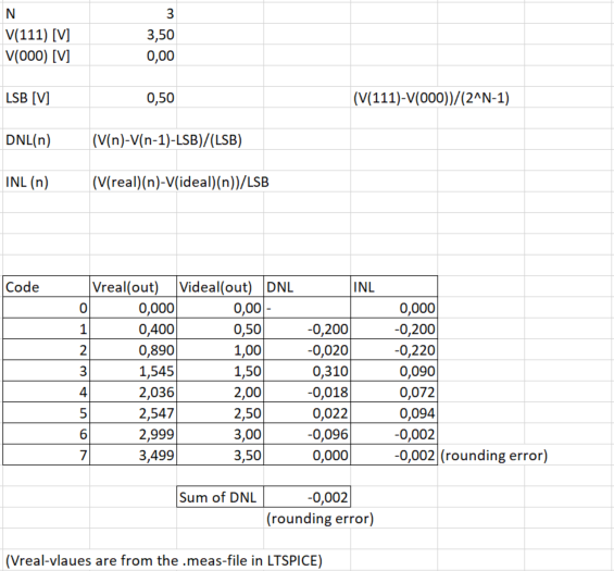
A 3 Bit DAC test was simulated in LTSPICE. The file was downloaded and the LTSPICE simulation was started. With different pulses on the different N-Mosfets the voltage vout changed over simulation time. The pulses are representing data values (numbers from 0 to 7). With the modified measurement .meas-file of the 4 Bit ADC/DAC the voltage levels at this 3 Bit DAC were measured. In the transfer curve we can see, that there are some errors in the output voltage. Different distances of the voltage levels are visible in the transfer curve. This is caused by the different values of resistors R1 to R8 in the .asc file. LSB - Least significant bit The LSB of the 3 Bit DAC was calculated with the first and last code. DNL - Differential non linearity Due to this different distances in the voltage levels we get a differential non linearity DNL what was calculated with the measured voltage levels over the .meas file. INL - Integral non lineatrity The integral of not linearity INL was also calculated via the measured values of the .meas file. All the calulations were made with Microsoft-Excel - a picture of the used formulas and results was added.  |
