Test for 4 Bit ADC and DAC
|
A 4 Bit ADC and DAC test can be simulated in LTSPICE. The files were downloaded and LTSpice simulation was started The output file size is limited by using the .save dialog option. A voltage source was added with a ramp from 0 V to 1 V with a rise time of 655µs The picture shows a ramp in put volrage and the DAC ramp output volrage over time. 16 steps can be seen. With a measurement statement the voltage levels were extracted. .Measure TRAN V0000 FIND V(Vout) AT=20u At 60us time the output of 0.0625 V is given for the code 0001 V0001: V(vout)=0.0625 at 6e-005 No error in the voltage level can be seen. It is an ideal ADC and DAC 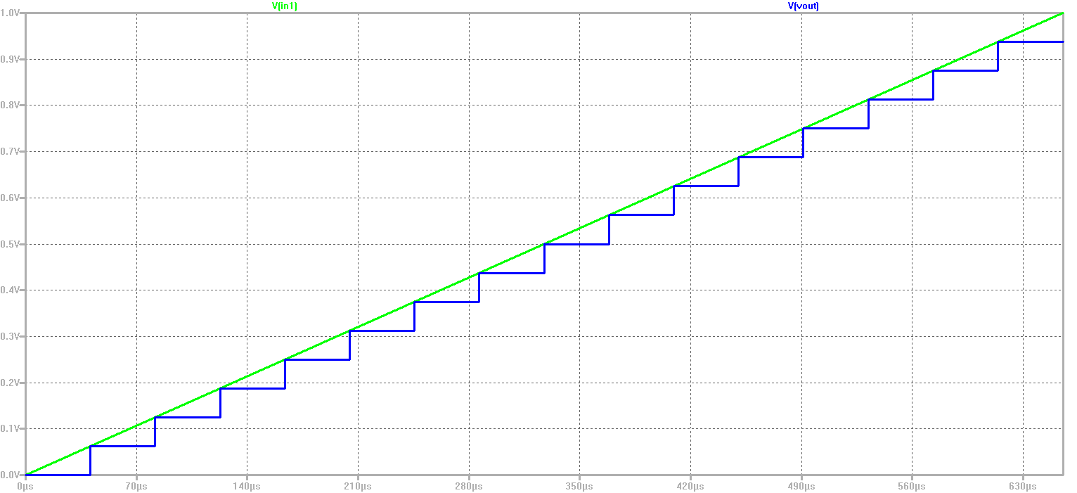 |
Calculation INL DNL of the 3 Bit DAC
|
At first a 3 Bit R2R DAC is simulated by LTSPICE. The output voltage can be seen in the lower picture. 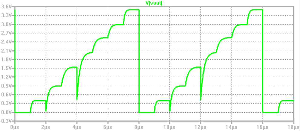 Based on this simulation the DNL and INL was calculated. Therefore at first a new measurement script was set up. This is the updated measurement script: .measure TRAN V0000 FIND V(Vout) AT = 0.95u .measure TRAN V0001 FIND V(Vout) AT = 1.95u .measure TRAN V0002 FIND V(Vout) AT = 2.95u .measure TRAN V0003 FIND V(Vout) AT = 3.95u .measure TRAN V0004 FIND V(Vout) AT = 4.95u .measure TRAN V0005 FIND V(Vout) AT = 5.95u .measure TRAN V0006 FIND V(Vout) AT = 6.95u .measure TRAN V0007 FIND V(Vout) AT = 7.95u Shortly before every transition, a voltage measurement was done. Here, the results of the measurements are listed: V0000: V(Vout)=5.23702e-013 at 9.5e-007 V0001: V(Vout)=0.399999 at 1.95e-006 V0002: V(Vout)=0.899042 at 2.95e-006 V0003: V(Vout)=1.54559 at 3.95e-006 V0004: V(Vout)=2.03594 at 4.95e-006 V0005: V(Vout)=2.54696 at 5.95e-006 V0006: V(Vout)=2.99917 at 6.95e-006 V0007: V(Vout)=3.49999 at 7.95e-006 From these results, it can be seen, that the simulated DAC isn't ideal. For instance, V0000 would be 0 V, if the DAC was an ideal one. Using the equations introduced in the lecture, now the INL and DNL is calculated.  The biggest part of the differential and integral non linearity is caused by the incorrect resistances. If all the resistances were equal to 100 Ohm, the failures would be close to zero. |