Interface ElectronicsLaboratory 01GroupC6, ***995, RADC and DAC LTSPICE Simulation |
Overview
- Install webpage template
- Download LTSPICE files
- Simulation Analysis
- Summary
Installation of webpage
- Download the template.zip file
- Go to directory InEl_P2019
- Unzip the file
- Copied directory 2019_GroupX to 2020_Group<C6<_;<Raza<
- In the directory copy the file: 2017_Group01_V00.html to 2020_Group<C6<_V1_<Raza<
- Edit with Notepad++: 2020_Group<C6<_V1_<Raza<
- Change the header, Change the footer, Made slide overview, Installation
Test for 4 Bit ADC and DAC
|
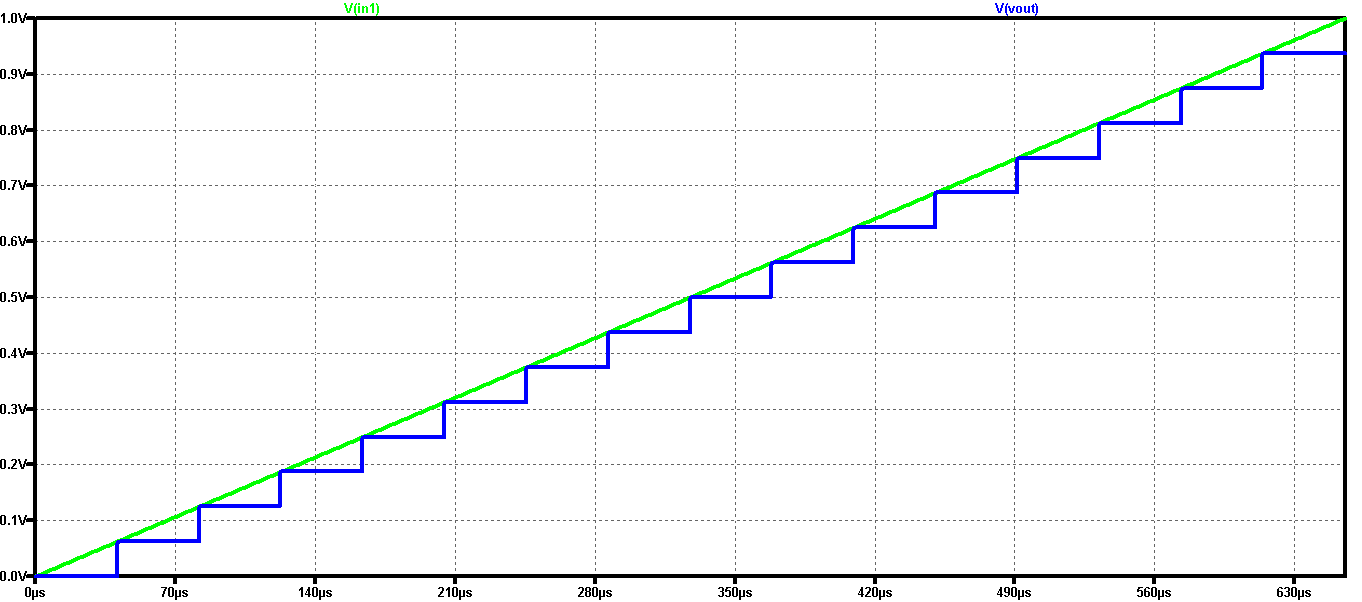
A 4 Bit ADC and DAC test can be simulated in LTSPICE. The files were downloaded and LTSPICE was started. The output file size can be limited by using the .save dialog option. A voltage cource was added with a ramp from 0 V to 1 V with a rise time of 655µs. The picture shows a ramp impact voltage and DAC ramp output voltage over 16 steps can be seen. With a measurement statement the voltage levels were extracted. .Measure TRAN V0000 FIND V(Vout) AT=20u At 60us time the output of 0.0625 V is given for the code 0001. V0001: V(Vout)=0.0625 at 6e-005 No error in the voltage level can be seen. It is an ideal ADC and DAC.  |
LTSPICE schematics
|
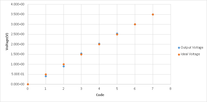
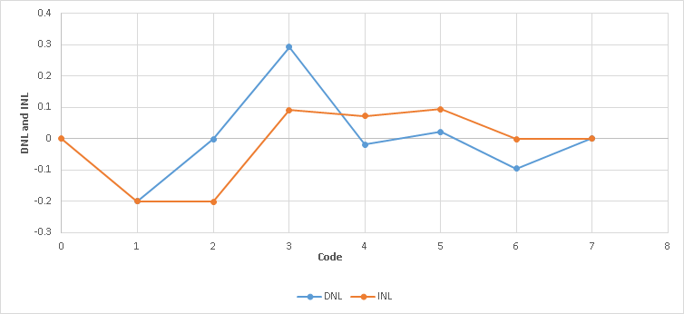
In this section, we will the real output voltages by using the .MEAS script of the LTSPICE. The resulting waveform is given below. After that, the DNL and INL values has been calculated manually and their graphs can be seen below.    |
Summary and Learning Outcomes
|
In this laboratory, I got a chance to learn how to code in HTML and I made my first web report. I tested the 4 bit DAC and ADC in LTSPICE and observed their outputs from the simulation. Then, I observed the difference between real and ideal output voltages. Later on, I calculated the DNL and INL values and plotted their outputs using microsoft Excel. During the implementation, I learned many new features of LTSPICE like executing the .MEAS script. I faced few challenges as well during the implementation. For example, the circuits were not showing in the browser. In order to solve this problem, I have to change the flag privacy.file_unique_origin to False. In short, this lab report prepared us for the incoming laboratories. After the completion of this report, I am more than ready to perform future tasks on LTSPICE and submit the reports using the HTML. |
Hochschule für angewandte Wissenschaften Kempten, Jörg Vollrath, Bahnhofstraße 61 · 87435 Kempten
Tel. 0831/25 23-0 · Fax 0831/25 23-104 · E-Mail: joerg.vollrath(at)fh-kempten.de
Impressum