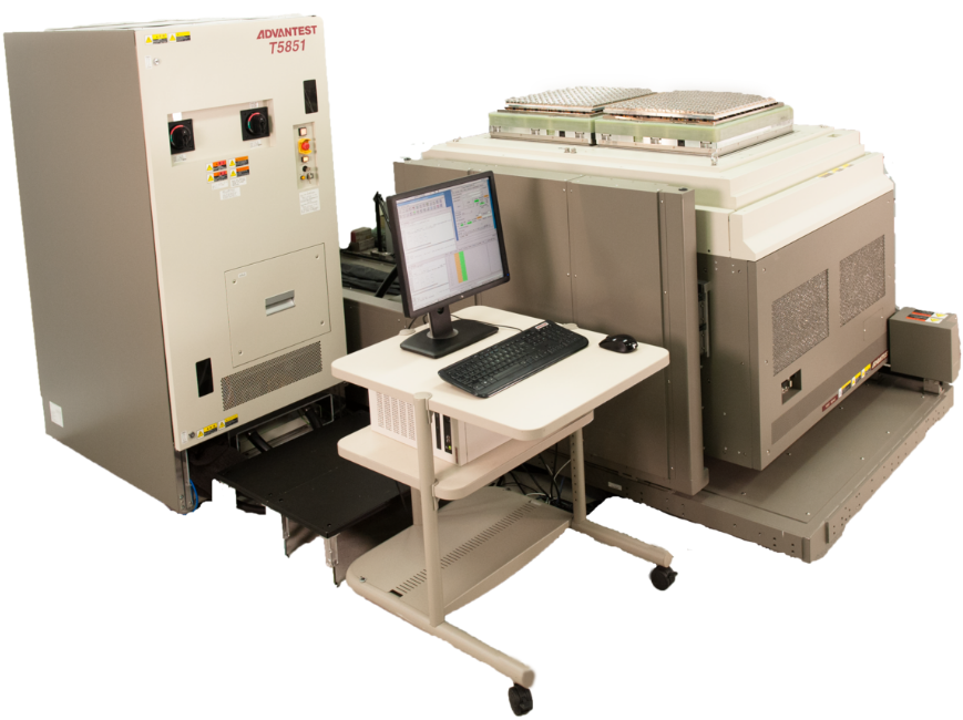
Memory tester and component handler
 |
|
Shown is a memory tester with a workstation and a test head at the left.
This test head can be inserted to the component handler station on the right. Similar test heads are available for a wafer probe station.
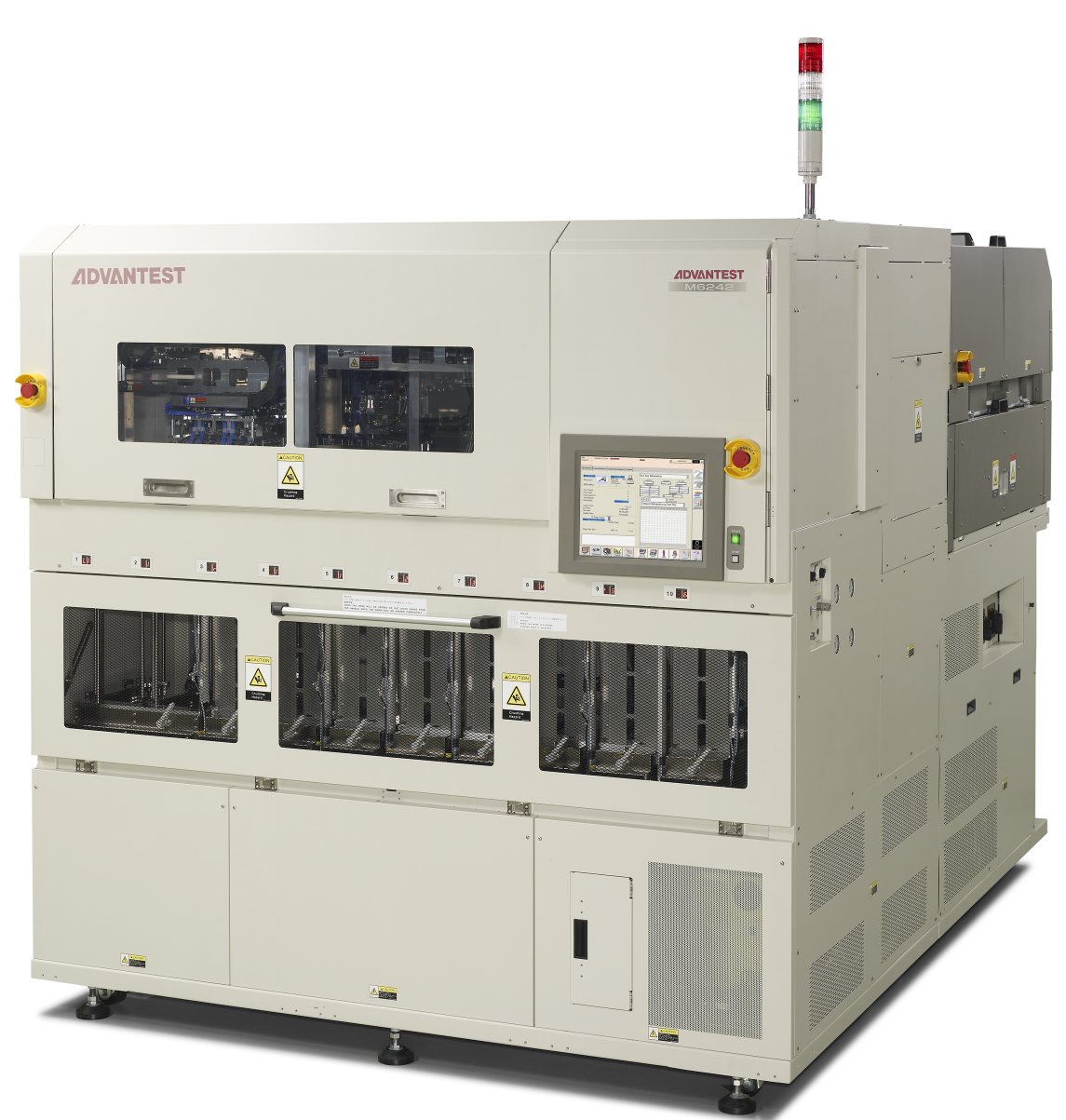
Memory testers for charcterization and wafer probing are provided by MOSAID, Advantest and Teradyne.
This test head can be inserted to the component handler station on the right. Similar test heads are available for a wafer probe station.
Memory testers for charcterization and wafer probing are provided by MOSAID, Advantest and Teradyne.
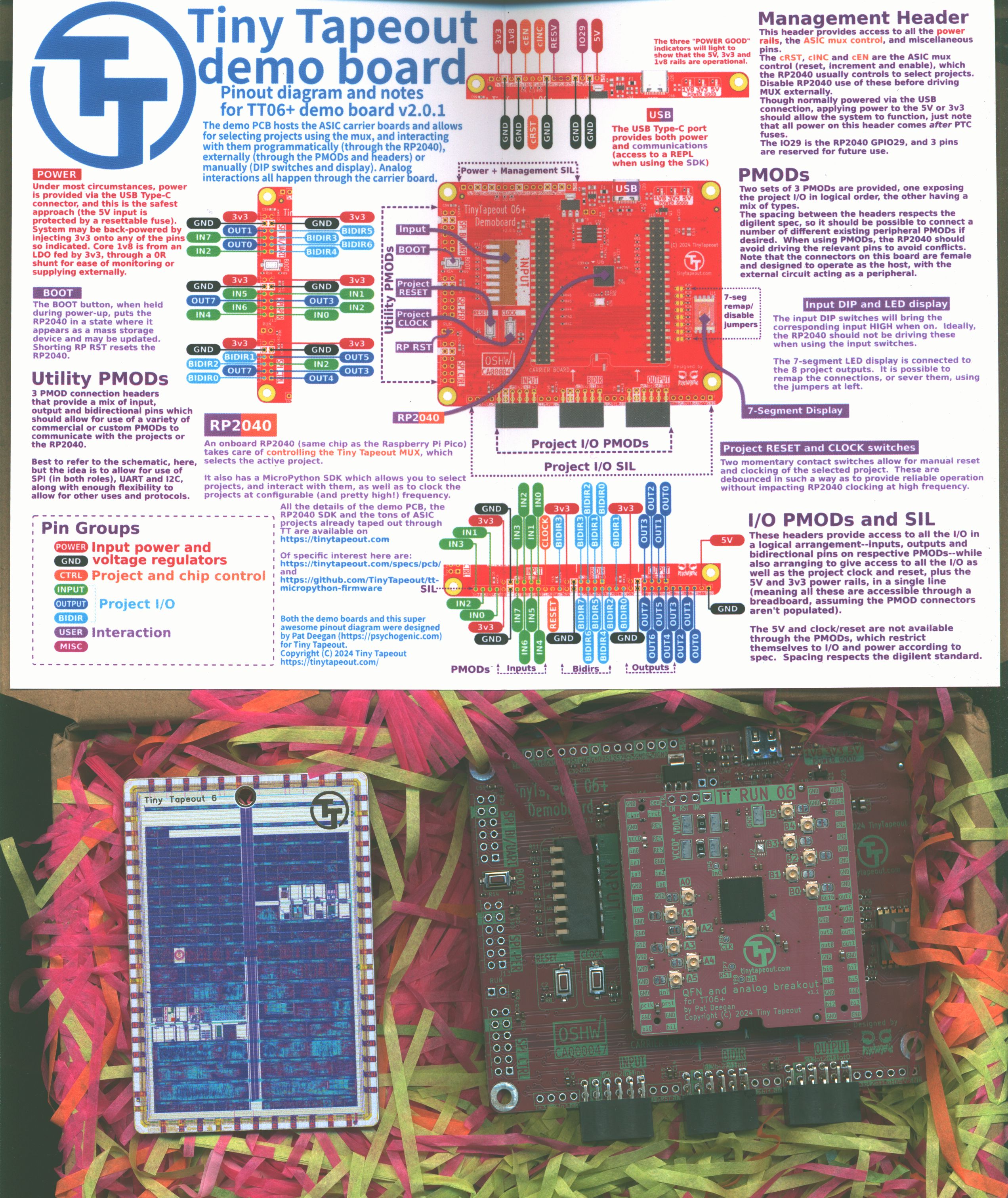
Evaluation platform
|
Tiny Tapeout Low cost easy entry chip design 482:1st order passive Sigma Delta ADC Joerg Vollrath https://tinytapeout.com/ |
|
Tiny Tapeout provides an easy way to get from a verilog description
to a digital electronic packaged chip at low cost (200..300.-$ 2025)
in 9 months.
There are 8 digital inputs, 8 digital outputs and 8 digital IOs available.
Additional area and analog pins are provided at higher costs and using a graphical layout tool.
The packaged TinyTapout TT06 chip with evaluation board is pictured on the right.
After cnnecting the board with USB to a PC a design can be selected via a web interface.
Documentation is provided via Github.
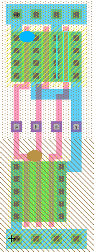
Layout and Defects
The layout influences the probability of shorts caused by defects |
|
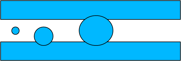
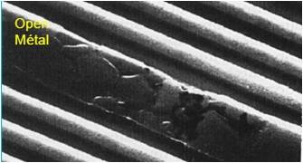
The picture shows a simplified model of defects on a layout.
A remaining metal1 particle shorts the drain and sourc of the upper left PFET.
A polysilicon particle shorts the polysilicon lines of the NFETs from inputs a and b.
A direct short of polysilicon lines from input a and c is not possible without involving polysilicon of input b.
This can have an impact on the necessary test pattern for the inputs.
Faults, Layout and Defect size
|
|
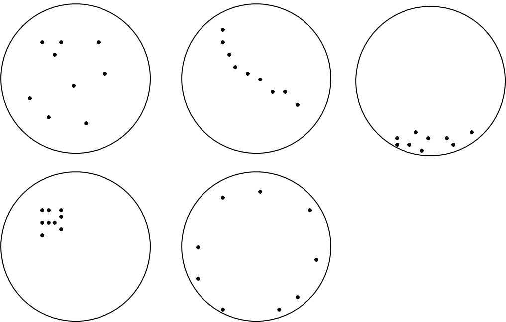
Defect wafer map
Same defect count can lead to different signatures
Defects and faults
Defects
|

|
FaultsS@0 stuck at 0 S@1 stuck at 1 Transition faults (TF) Coupling faults (CF) Realistic fault coverage |
Modeling Defects
|
Hard defects Truth table
|
|
|
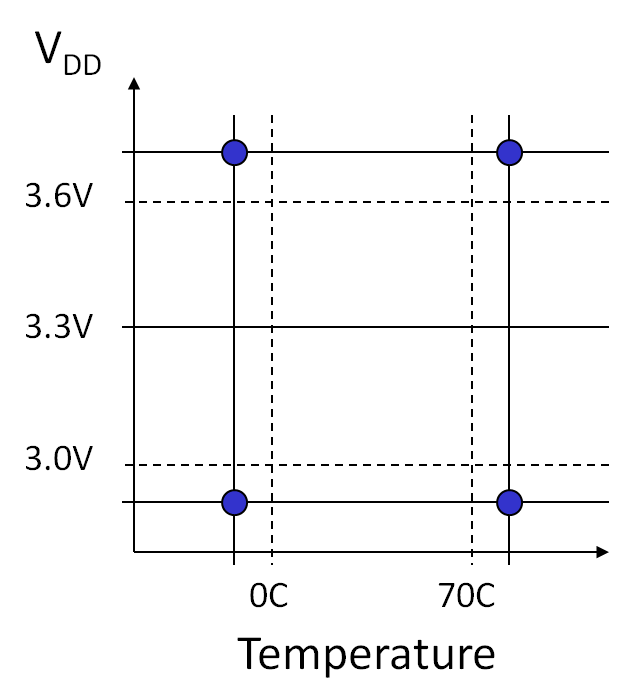
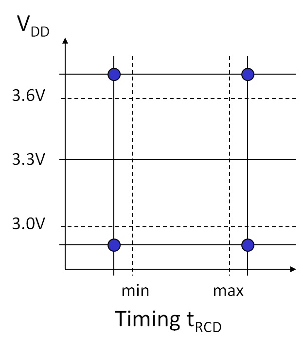
Timing delay fault

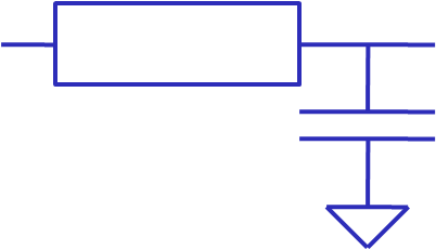
Guard Band
|
|
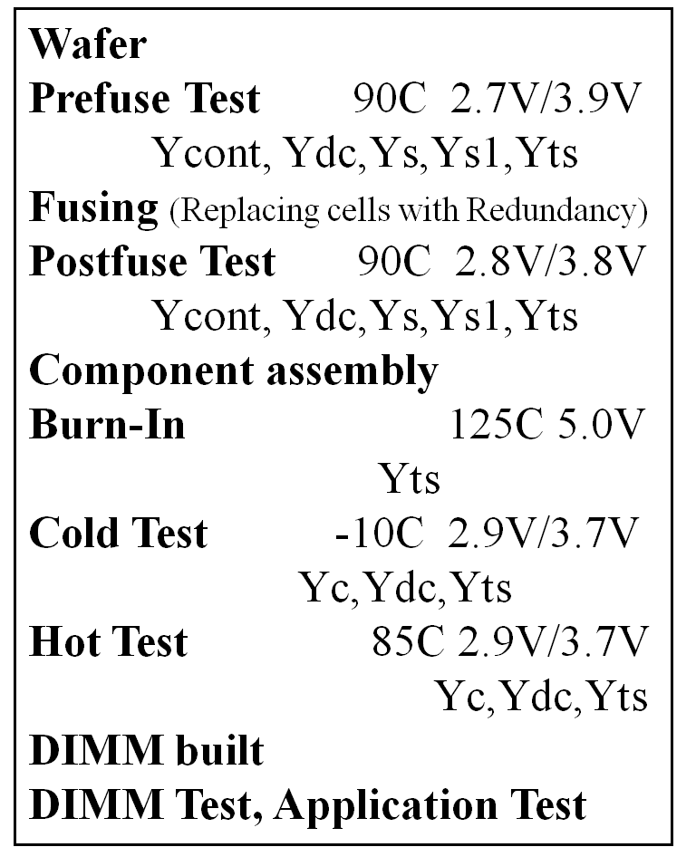
Memory test flow
|
|