Power and Speed
|
|
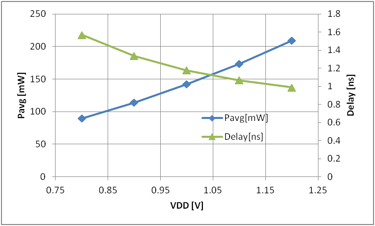
Performance of a semiconductor process can be measured using a ring oscillator.
The ring oscillator connects the output of an odd series of inverters with the input creating an unstable feedback.
The oscillator frequency is limited by the propagation delay of the inverters.
This measures the RDSon, Cin and ft.
The ring oscillator connects the output of an odd series of inverters with the input creating an unstable feedback.
The oscillator frequency is limited by the propagation delay of the inverters.
This measures the RDSon, Cin and ft.
Dynamic power peaks and currents
|
DRAM dynamic read current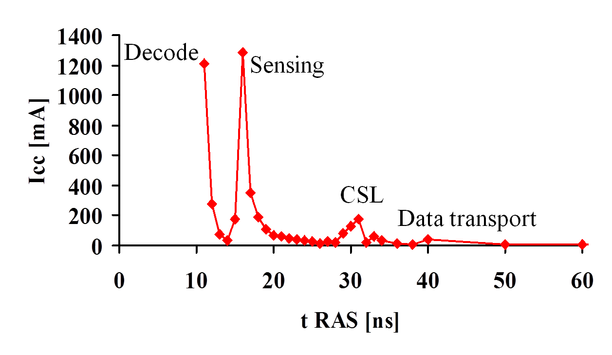
|
Ring oscillator power buffering with bypass capacitors
Simulation: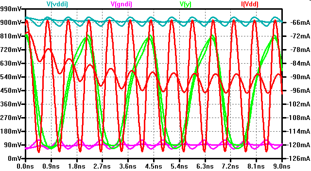
|
A ring oscillator shows the performance of a given semiconductor technology.
A 50 nm simulation shows a frequency of 500 MHz.
Series resistance in the power lines limits the voltage swing between 80 mV and 900 mV.
Average current is 93 mA.
The voltage level of gnd and vdd shows a ringing due to changing IDD.
Bypass capacitors can reduce the swing on the power lines, given more stable operation.
Not used area on chip can be filled with capacitance.
Real bypass capacitors
Frequency response of power capacitances: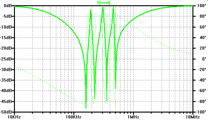
|
A real capacitance has a parasitic resistance and inductance.
There is a limited bandwidth for supply voltage stabilization.
A combination of many capacitances with optimized resistance and inductance is needed.
There is a limited bandwidth for supply voltage stabilization.
A combination of many capacitances with optimized resistance and inductance is needed.
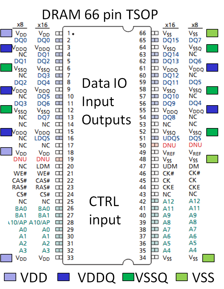
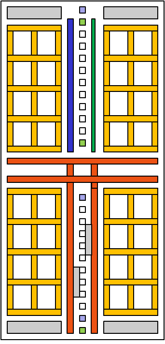
Power grid: DRAM example
|
|
There are separate power supply pins for the data input and outputs (IO).
The number of power pins is proportional to the number of IOs.
There are separate grids for digital and analog circuits.
Horizontal and vertical lines are connected to a grid and provide power.
The block diagram shows different voltages in different colors in different areas.
Voltage pumps and regulators are shown in grey.
A bandgap reference circuit provides temperature and voltage independent voltages.
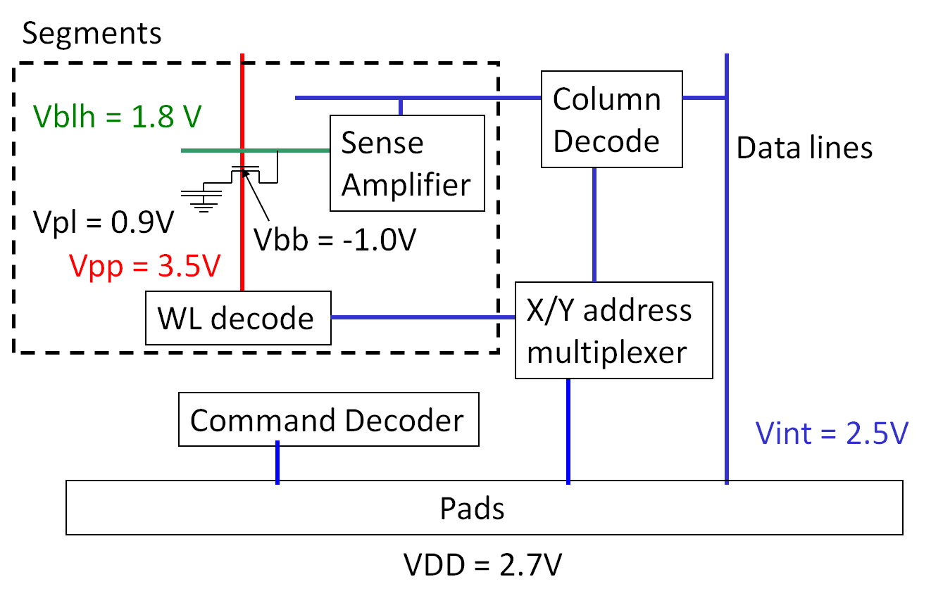
Power on sequence: DRAM
|
A low array voltage is used to save power.
A negative back bias is needed reducing memory cell leakage current.
A high voltage Vpp gives the select transistor overdrive to store the full Vblh level in the memory cell.
Vint is optimized for speed and to be able to drive the IOs.
A high current peak, when power is turned on, has to be avoided.
All capacitances will be charged up at power up.
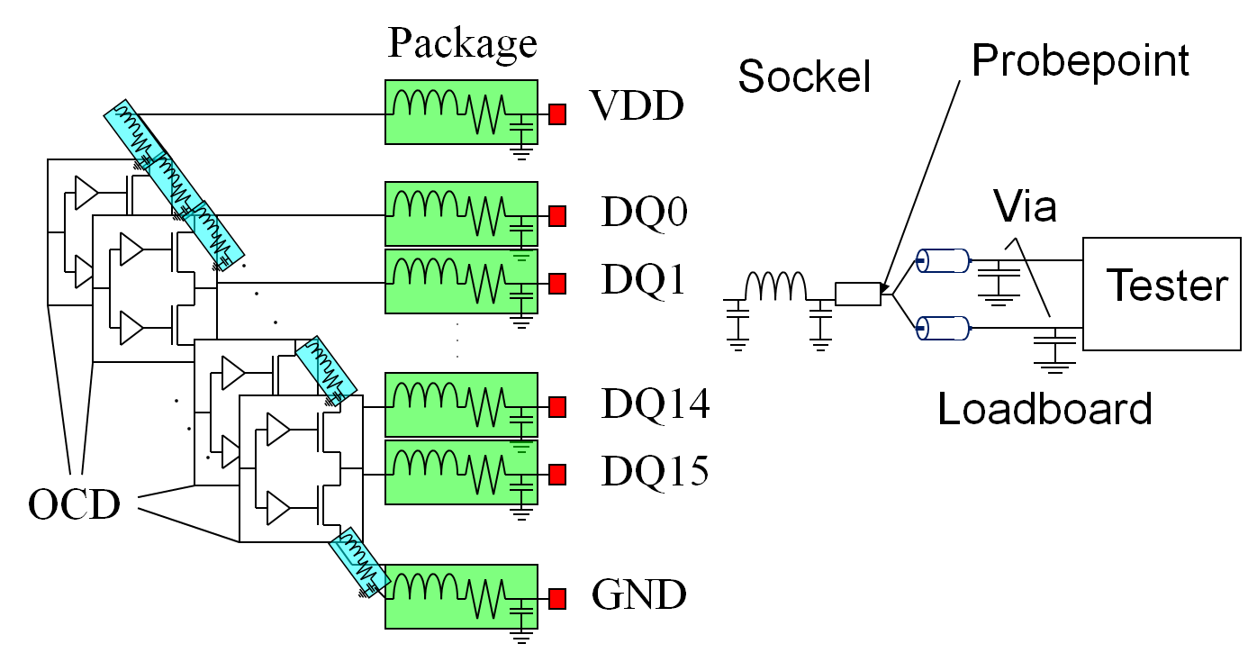
Power system model
|
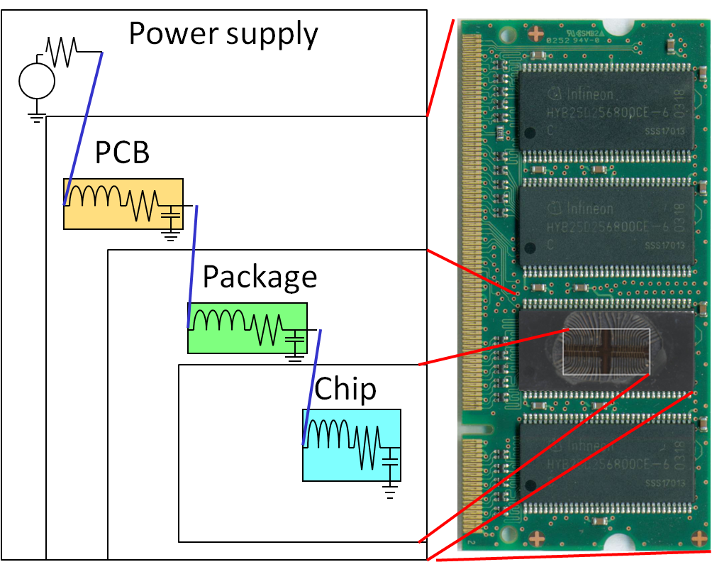 |
Memory chip package
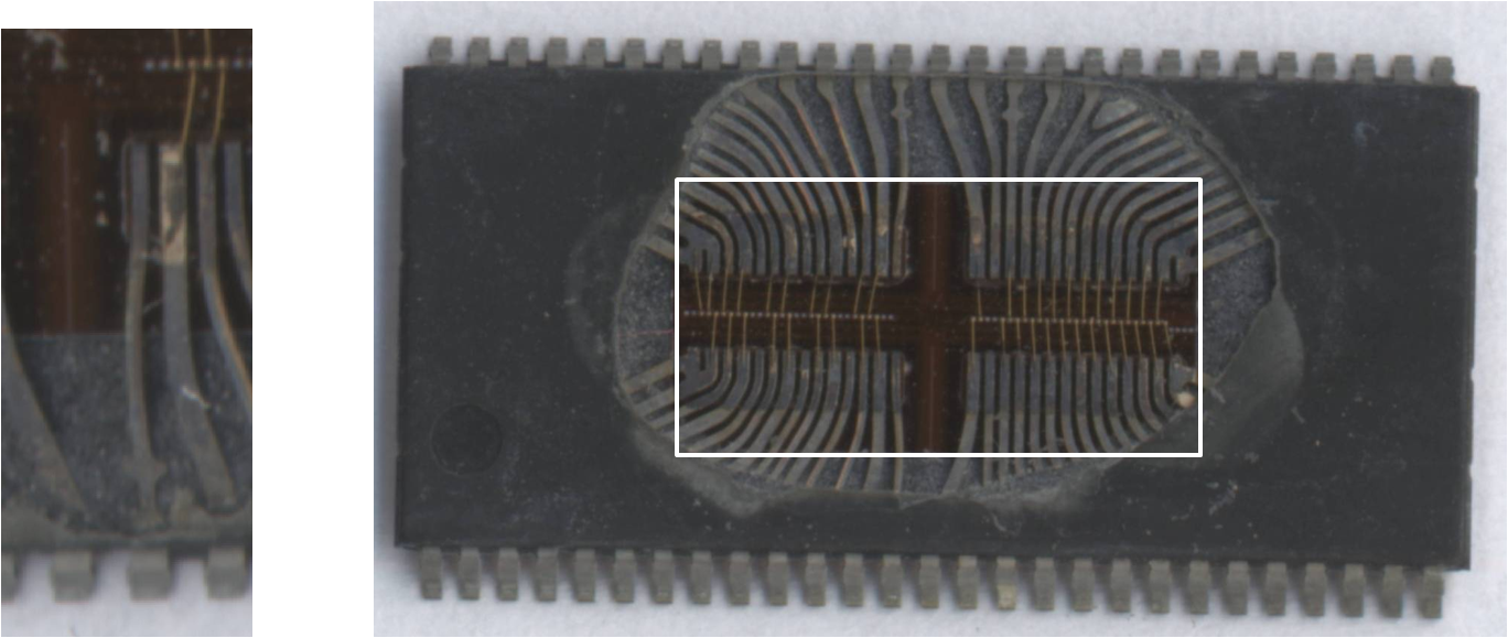
This is a TSOP5 package used around 2005 for DRAM memories.
Nowadays memories use bga packages.
The package is smaller and has better high speed performance. It is more expensive than a TSOP package. Test and failure analysis is more difficult.
Nowadays memories use bga packages.
The package is smaller and has better high speed performance. It is more expensive than a TSOP package. Test and failure analysis is more difficult.
CLK Distribution: H-Tree and clock domains
H Tree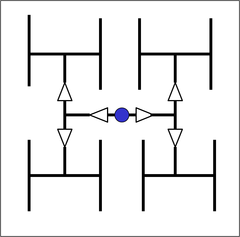
|
System on chip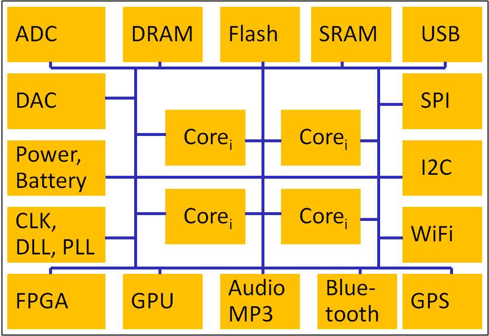
|
Microprocessors have one central clock distributed via a balanced or unbalanced H-tree.
Systems on chip have many blocks with local clocks.
Communication is done via serial bus between clock domains.
Divide and conquer.
Systems on chip have many blocks with local clocks.
Communication is done via serial bus between clock domains.
Divide and conquer.
Package and Pads
|
Dual in line (DIL) Thin small outline (TSOP) 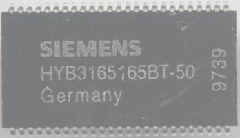 Ball grid array (BGA) 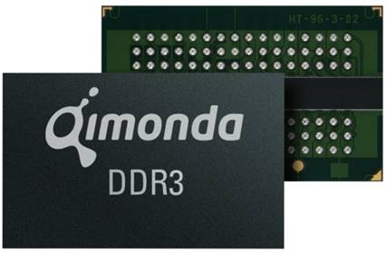 |
Package parasitics
Bond wiresGold bond wires connect the chip pads with metal lead frame. Thermal coupling is also achieved with bond wires and lead frame. Model: Inductance Capacitance Resistance |
 |
SPICE simulation and measurement
IO pads and pins in VHDL
User constraint file (.ucf)
|
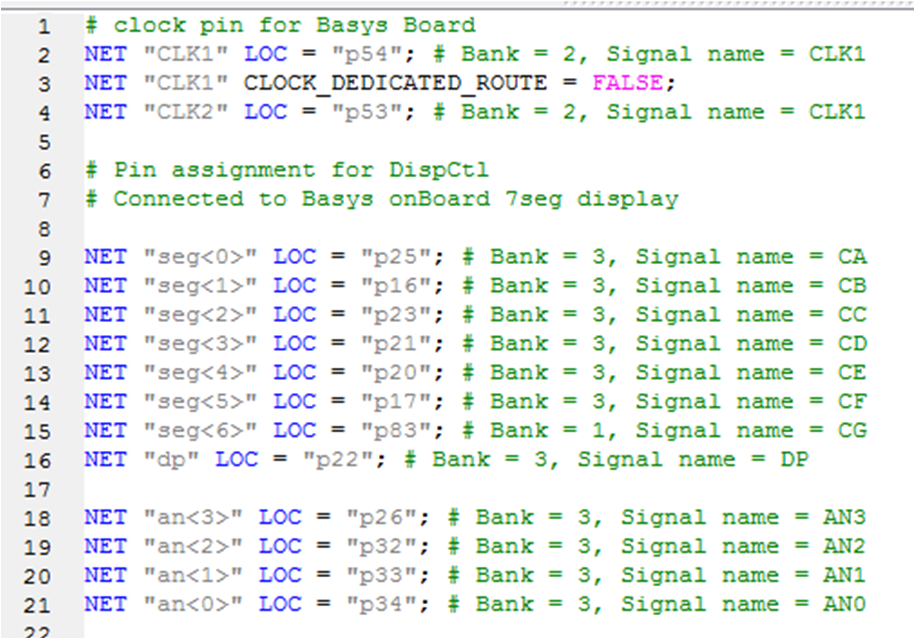
|
References
Laboratory: TinyFPGA2018 TinyFPGA
Electric libraries:
muddpads13_ami05.jelib
pads4u.jelib
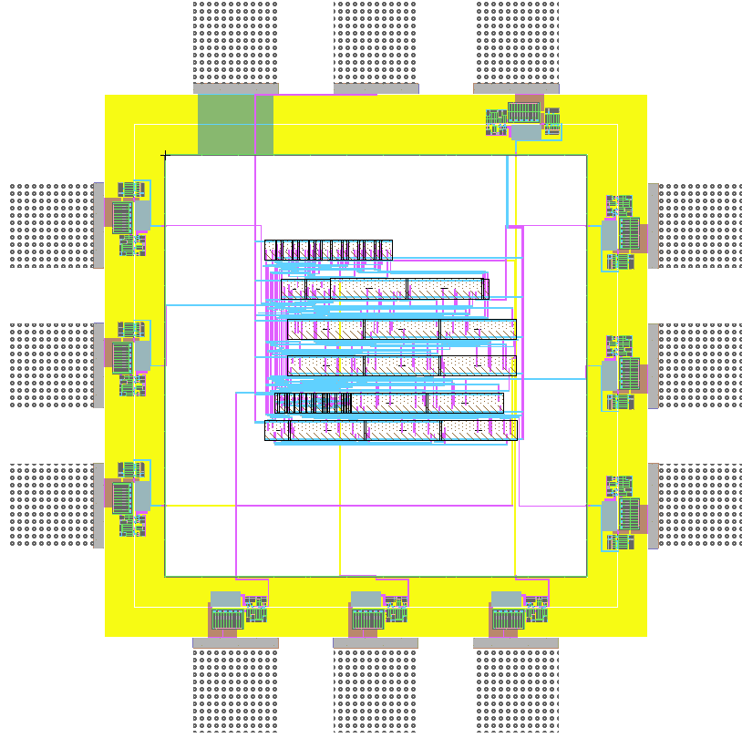
Electric: Tools -> Generation -> Pad frame generator
A configuration file (*.arr) allows automatic pad generation. Wiring can then be done with the Sea of gates route.
In the user manual an example is provided.
This example shows the pad frame not the active area to limit minimum chip size.
Alignment marks and labels for chip identification are missing.
Multiple chips are put on one reticle with a distance of 200 µm for sawing (dicing) to separate the chips.
Test structures are placed in this space to be able to monitor process performance.
MOSIS 0.35 µm IO Pads
MOSIS 0.35 µm IO Pads