Guided Laboratory 2020: Serial gray code to binary code
Joerg VollrathLaboratory Instructions
A folding pipeline ADC generates a serial gray code bit stream starting with MSB and ending with LSB.
A digital circuit converting a 16 bit serial bit stream should be designed.
8 bit folding Pipeline ADC LTSPICE circuit
In Interface electronics a circuit FoldingPipelineTest.asc uses Shift8Gray.asc for conversion.
In this laboratory a digital circuit converting a 16 bit serial bit stream should be designed.
General specification
- Inputs
- C3 initiate a new serial parallel conversion
- C2 control new GD data acquisition and shift by one position of the input
- GD Data: MSB comes first, LSB comes in last.
- Gray code to binary
- An EXOR operating with the previous bit converts gray to binary
- Outputs
- D0 to D15 are the final values of the parallel output
Conversion table
| Decimal | Binary | Gray Code |
| 0 | 000 | 000 |
| 1 | 001 | 001 |
| 2 | 010 | 011 |
| 3 | 011 | 010 |
| 4 | 100 | 110 |
| 5 | 101 | 111 |
| 6 | 110 | 101 |
| 7 | 111 | 100 |
Example conversion of 3 bits: '4' decimal, '100' binary, '110' gray
Specification:
First C3 edge: Transfer data of shift register to output
C2 edge: GD transfer to first shift bit
C2 edge: D0 exor GD transfer and shift bits
A schematic looks like this:
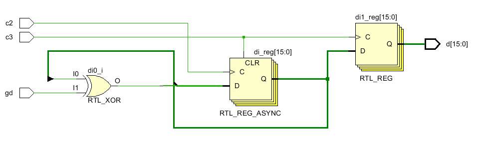
Schematic created with Vivado: 'RTL Analysis', 'Schematic'.
Xilinx Webpack ISE 14.7 running in a virtual machine was used with Spartan 6 device for converting behavioral VHDL to structural VHDL.
Xilinx Vivado was used for simulation. Unfortunately AnalyzeJS.html supports not the Spartan 7 output.
VHDL Synthesis Story
- Write VHDL description
- Write VHDL test bench and simulate
- Generate structural VHDL and transfer it via AnalyzeJS.html to Electric
- In a Electric generate a layout using Silicon Compiler.
VHDL code
entity SGrayBinary is
       port   (
          c3, c2, gd: in std_logic;
          d: out std_logic_vector(15 downto 0)
       );
    end entity SGrayBinary;

    architecture Behavioral of SGrayBinary is
    signal di:std_logic_vector(15 downto 0);
    signal di1:std_logic_vector(15 downto 0);
	 signal gdx:std_logic;
	 begin

         process(c2,c3)
         begin
			  if (c3 = '1') then
			      di <= "0000000000000000";
		     elsif  rising_edge(c2) then
               di <= di(14 downto 0) & (di(0) xor gd);
           end if;
         end process;

         process(c3)
         begin
			  if  rising_edge(c3) then
               di1 <= di;
           end if;
         end process;
			d <= di1;

    end architecture Behavioral;
Xilinx Webpack 14.7: Synthesize - XST - Generate Post-Synthesis Simulation Model.
Vivado: After synthesis run Tcl console command: 'write_vhdl <filename>' to get a structural post synthesis description for AnalyzeJS.html.
Test
3 bit streams are generated to check for a correct output.
ENTITY TestSGrayBinary IS
END TestSGrayBinary;

ARCHITECTURE behavior OF TestSGrayBinary IS

    -- Component Declaration for the Unit Under Test (UUT)

    COMPONENT SGrayBinary
    PORT(
         c3 : IN  std_logic;
         c2 : IN  std_logic;
         gd : IN  std_logic;
         d : OUT  std_logic_vector(15 downto 0)
        );
    END COMPONENT;


   --Inputs
   signal c3 : std_logic := '0';
   signal c2 : std_logic := '0';
   signal gd : std_logic := '0';

 	--Outputs
   signal d : std_logic_vector(15 downto 0);

   -- clk period
   constant cx_period : time := 10 ns;

BEGIN

   -- Instantiate the Unit Under Test (UUT)
   uut: SGrayBinary PORT MAP (
          c3 => c3,
          c2 => c2,
          gd => gd,
          d => d
        );

   -- Clock process definitions
   c2_process :process
   begin
		c2 <= '0';	wait for cx_period;
		c2 <= '1';	wait for cx_period;
   end process;

   c3_process :process
   begin
		c3 <= '0'; 	wait for cx_period/4;
		c3 <= '1';	wait for cx_period/4;
		c3 <= '0';	wait for cx_period/2 + cx_period * 31;
   end process;

   -- Stimulus process
   stim_proc: process
   begin
     -- grey code 1100 0100 0100 1000
	 -- binary    1000 0111 1000 1111
	 -- hex         8   7    8    F
      gd <= '1'; wait for cx_period * 2;
      gd <= '1'; wait for cx_period * 2;
      gd <= '0'; wait for cx_period * 2;
      gd <= '0'; wait for cx_period * 2;
      gd <= '0'; wait for cx_period * 2;
      gd <= '1'; wait for cx_period * 2;
      gd <= '0'; wait for cx_period * 2;
      gd <= '0'; wait for cx_period * 2;
      gd <= '0'; wait for cx_period * 2;
      gd <= '1'; wait for cx_period * 2;
      gd <= '0'; wait for cx_period * 2;
      gd <= '0'; wait for cx_period * 2;
      gd <= '1'; wait for cx_period * 2;
      gd <= '0'; wait for cx_period * 2;
      gd <= '0'; wait for cx_period * 2;
      gd <= '0'; wait for cx_period * 2;

     -- grey code 0010 1001 0011 0100
     -- binary    0011 0001 1101 1000
     -- hex         3   1    D    8
      gd <= '0'; wait for cx_period * 2;
      gd <= '0'; wait for cx_period * 2;
      gd <= '1'; wait for cx_period * 2;
      gd <= '0'; wait for cx_period * 2;
      gd <= '1'; wait for cx_period * 2;
      gd <= '0'; wait for cx_period * 2;
      gd <= '0'; wait for cx_period * 2;
      gd <= '1'; wait for cx_period * 2;
      gd <= '0'; wait for cx_period * 2;
      gd <= '0'; wait for cx_period * 2;
      gd <= '1'; wait for cx_period * 2;
      gd <= '1'; wait for cx_period * 2;
      gd <= '0'; wait for cx_period * 2;
      gd <= '1'; wait for cx_period * 2;
      gd <= '0'; wait for cx_period * 2;
      gd <= '0'; wait for cx_period * 2;

      -- grey code 0101 1011 1011 1100
      -- binary    0110 1101 0010 1000
      -- hex         6   D     2    8
      gd <= '0'; wait for cx_period * 2;
      gd <= '1'; wait for cx_period * 2;
      gd <= '0'; wait for cx_period * 2;
      gd <= '1'; wait for cx_period * 2;
      gd <= '1'; wait for cx_period * 2;
      gd <= '0'; wait for cx_period * 2;
      gd <= '1'; wait for cx_period * 2;
      gd <= '1'; wait for cx_period * 2;
      gd <= '1'; wait for cx_period * 2;
      gd <= '0'; wait for cx_period * 2;
      gd <= '1'; wait for cx_period * 2;
      gd <= '1'; wait for cx_period * 2;
      gd <= '1'; wait for cx_period * 2;
      gd <= '1'; wait for cx_period * 2;
      gd <= '0'; wait for cx_period * 2;
      gd <= '0'; wait for cx_period * 2;

      wait;
   end process;
END;
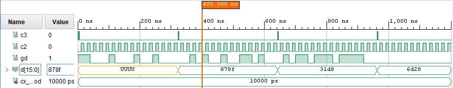
Vivado simulation
In the Vivado simulation 3 correct 16-bit output values d[15:0] can be seen.
It takes 16 clock cycles C2 to generate a new output value.
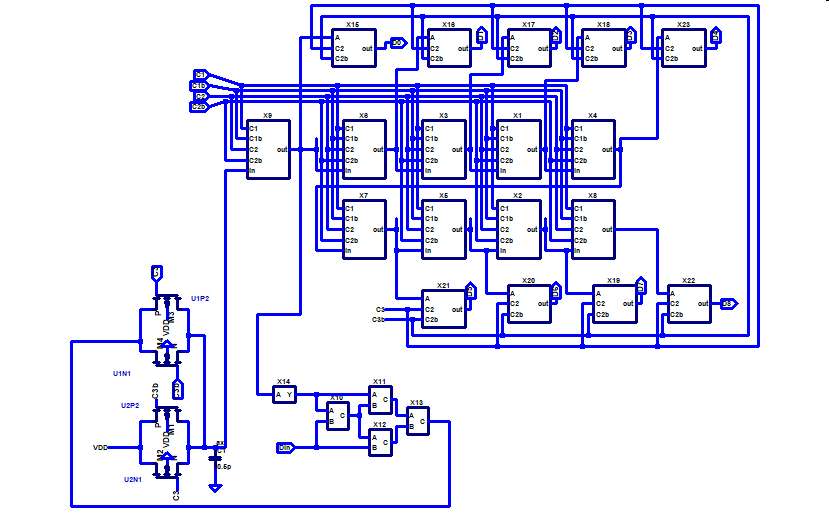
Synthesis of layout with Electric
Vivado:
After doing 'Synthesis - Open synthesized Desing' a synthesized vhd file is generated.
In Vivado a structural VHDL was the generated using TCL command window: write_vhdl <filename>.
The file is saved in a directory
Unfortunately AnalyzeJS.html does not support Vivado Spartan 7 devices yet.
In Xilinx Wepack a structural VHDL was the generated: SGrayBinary_synthesis.vhd
This file was inserted into AnalyzeJS.html.
After pressing 'Process VHDL for Electric (Type: BIT)' an Electric compatible VHDL is generated.
Start Electric and load the librarys sclib.jelib. A new library (File - New library) and cell (Cell - New Cell) view: 'VHDL' and name: 'SGrayBinary' is created.
The 'SGrayBinary' entity and architecture from AnalyzeJS.html are inserted.
The ':="X"' for c3, c2 and gd in the entity part is removed.
The last semicolon after d__15 is removed.
The components are inserted into the architecture:
architecture Structure of SGrayBinary is

component BUFGP port ( I: in BIT;O: out BIT);
 end component;
component FDC port ( C, CLR,D: in BIT;Q: out BIT);
 end component;
component FD port ( C, D: in BIT;Q: out BIT);
 end component;
component OBUF port ( I: in BIT;O: out BIT);
 end component;
component IBUF port ( I: in BIT;O: out BIT);
 end component;
component LUT26 port ( I0,I1: in BIT;O: out BIT);
 end component;


signal c3_IBUF_BUFG_0 : BIT;
Since there is no cell BUFG available it is replaced with BUFGP and the O and I lines are sorted correctly.There is no cell FD available, so a new cell was created.
The result is: SGrayBinary_synthesisElectric.vhd Then a layout is generated with 'Silicon Compiler' and LTSPICE code is added.
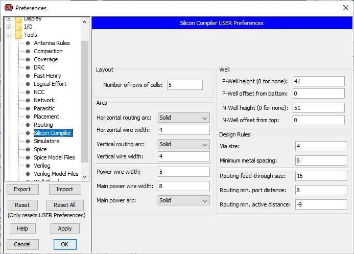
Be sure to select a M1 line in any layout cell to avoid error: "SC Maker cannot find Horizontal Arc Metal-1 in technology artwork"
In "File - Preferences - Tools - Silicon Compiler" the number of rows can be changed.
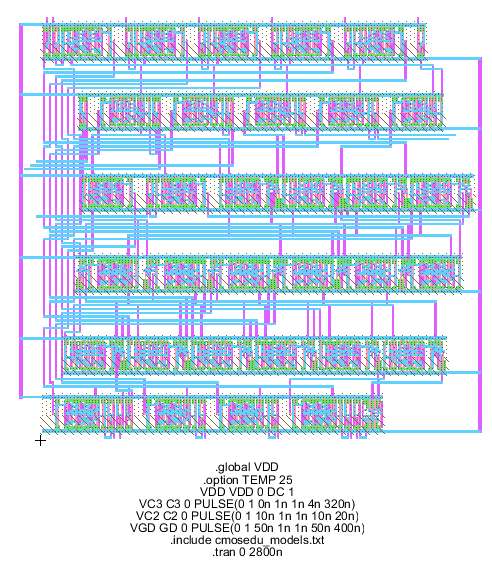
 Synthesized layout
Add LTSPICE simulation code to layout.

.global VDD
.option TEMP 25
VDD VDD 0 DC 1
VC3 C3 0 PULSE(0 1 0n 1n 1n 4n 320n)
VC2 C2 0 PULSE(0 1 10n 1n 1n 10n 20n)
VGD GD 0 PULSE(0 1 50n 1n 1n 50n 400n)
.include cmosedu_models.txt
.tran 0 2800n
Input vectors for TestJS.html
Xilinx has asynchronous reset with C3. FDC in sclib has synchronous reset.
C2 has to do a clock cycle while C3 active.
Use TestJS to create LTSPICE simulation commands.
Paste the test vectors into the input field and 'Generate analysis request'.
C2,C3,GD;xD15,xD14,xD13,xD12,xD11,xD10,xD9,xD8,xD7,xD6,xD5,xD4,xD3,xD2,xD1,xD0;COMMENT
 0, 1, 0; 0,0,0,0,0,0,0,0,0,0,0,0,0,0,0,0;
 1, 1, 0; 0,0,0,0,0,0,0,0,0,0,0,0,0,0,0,0; Reset
 0, 0, 1; 0,0,0,0,0,0,0,0,0,0,0,0,0,0,0,0;
 1, 0, 1; 0,0,0,0,0,0,0,0,0,0,0,0,0,0,0,0; GD "1" 15
 0, 0, 1; 0,0,0,0,0,0,0,0,0,0,0,0,0,0,0,0;
 1, 0, 1; 0,0,0,0,0,0,0,0,0,0,0,0,0,0,0,0; GD "1"
 0, 0, 0; 0,0,0,0,0,0,0,0,0,0,0,0,0,0,0,0;
 1, 0, 0; 0,0,0,0,0,0,0,0,0,0,0,0,0,0,0,0; GD "0"
 0, 0, 0; 0,0,0,0,0,0,0,0,0,0,0,0,0,0,0,0;
 1, 0, 0; 0,0,0,0,0,0,0,0,0,0,0,0,0,0,0,0; GD "0"
 0, 0, 0; 0,0,0,0,0,0,0,0,0,0,0,0,0,0,0,0;
 1, 0, 0; 0,0,0,0,0,0,0,0,0,0,0,0,0,0,0,0; GD "0" 11
 0, 0, 1; 0,0,0,0,0,0,0,0,0,0,0,0,0,0,0,0;
 1, 0, 1; 0,0,0,0,0,0,0,0,0,0,0,0,0,0,0,0; GD "1"
 0, 0, 0; 0,0,0,0,0,0,0,0,0,0,0,0,0,0,0,0;
 1, 0, 0; 0,0,0,0,0,0,0,0,0,0,0,0,0,0,0,0; GD "0"
 0, 0, 0; 0,0,0,0,0,0,0,0,0,0,0,0,0,0,0,0;
 1, 0, 0; 0,0,0,0,0,0,0,0,0,0,0,0,0,0,0,0; GD "0"
 0, 0, 0; 0,0,0,0,0,0,0,0,0,0,0,0,0,0,0,0;
 1, 0, 0; 0,0,0,0,0,0,0,0,0,0,0,0,0,0,0,0; GD "0" 7
 0, 0, 1; 0,0,0,0,0,0,0,0,0,0,0,0,0,0,0,0;
 1, 0, 1; 0,0,0,0,0,0,0,0,0,0,0,0,0,0,0,0; GD "1"
 0, 0, 0; 0,0,0,0,0,0,0,0,0,0,0,0,0,0,0,0;
 1, 0, 0; 0,0,0,0,0,0,0,0,0,0,0,0,0,0,0,0; GD "0"
 0, 0, 0; 0,0,0,0,0,0,0,0,0,0,0,0,0,0,0,0;
 1, 0, 0; 0,0,0,0,0,0,0,0,0,0,0,0,0,0,0,0; GD "0"
 0, 0, 1; 0,0,0,0,0,0,0,0,0,0,0,0,0,0,0,0;
 1, 0, 1; 0,0,0,0,0,0,0,0,0,0,0,0,0,0,0,0; GD "1" 3
 0, 0, 0; 0,0,0,0,0,0,0,0,0,0,0,0,0,0,0,0;
 1, 0, 0; 0,0,0,0,0,0,0,0,0,0,0,0,0,0,0,0; GD "0"
 0, 0, 0; 0,0,0,0,0,0,0,0,0,0,0,0,0,0,0,0;
 1, 0, 0; 0,0,0,0,0,0,0,0,0,0,0,0,0,0,0,0; GD "0"
 0, 0, 0; 0,0,0,0,0,0,0,0,0,0,0,0,0,0,0,0;
 1, 0, 0; 0,0,0,0,0,0,0,0,0,0,0,0,0,0,0,0; GD "0"
 0, 1, 0; 0,0,0,0,0,0,0,0,0,0,0,0,0,0,0,0;
 1, 1, 0; 1,0,0,0,0,1,1,1,1,0,0,0,1,1,1,1; Reset expect 878f
 0, 0, 0; 1,0,0,0,0,1,1,1,1,0,0,0,1,1,1,1;
 1, 0, 0; 1,0,0,0,0,1,1,1,1,0,0,0,1,1,1,1; GD "0" 15
 0, 0, 0; 1,0,0,0,0,1,1,1,1,0,0,0,1,1,1,1;
 1, 0, 0; 1,0,0,0,0,1,1,1,1,0,0,0,1,1,1,1; GD "0"
 0, 0, 1; 1,0,0,0,0,1,1,1,1,0,0,0,1,1,1,1;
 1, 0, 1; 1,0,0,0,0,1,1,1,1,0,0,0,1,1,1,1; GD "1"
 0, 0, 0; 1,0,0,0,0,1,1,1,1,0,0,0,1,1,1,1;
 1, 0, 0; 1,0,0,0,0,1,1,1,1,0,0,0,1,1,1,1; GD "0"
 0, 0, 1; 1,0,0,0,0,1,1,1,1,0,0,0,1,1,1,1;
 1, 0, 1; 1,0,0,0,0,1,1,1,1,0,0,0,1,1,1,1; GD "1" 11
 0, 0, 0; 1,0,0,0,0,1,1,1,1,0,0,0,1,1,1,1;
 1, 0, 0; 1,0,0,0,0,1,1,1,1,0,0,0,1,1,1,1; GD "0"
 0, 0, 0; 1,0,0,0,0,1,1,1,1,0,0,0,1,1,1,1;
 1, 0, 0; 1,0,0,0,0,1,1,1,1,0,0,0,1,1,1,1; GD "0"
 0, 0, 1; 1,0,0,0,0,1,1,1,1,0,0,0,1,1,1,1;
 1, 0, 1; 1,0,0,0,0,1,1,1,1,0,0,0,1,1,1,1; GD "1"
 0, 0, 0; 1,0,0,0,0,1,1,1,1,0,0,0,1,1,1,1;
 1, 0, 0; 1,0,0,0,0,1,1,1,1,0,0,0,1,1,1,1; GD "0" 7
 0, 0, 0; 1,0,0,0,0,1,1,1,1,0,0,0,1,1,1,1;
 1, 0, 0; 1,0,0,0,0,1,1,1,1,0,0,0,1,1,1,1; GD "0"
 0, 0, 1; 1,0,0,0,0,1,1,1,1,0,0,0,1,1,1,1;
 1, 0, 1; 1,0,0,0,0,1,1,1,1,0,0,0,1,1,1,1; GD "1"
 0, 0, 1; 1,0,0,0,0,1,1,1,1,0,0,0,1,1,1,1;
 1, 0, 1; 1,0,0,0,0,1,1,1,1,0,0,0,1,1,1,1; GD "1"
 0, 0, 0; 1,0,0,0,0,1,1,1,1,0,0,0,1,1,1,1;
 1, 0, 0; 1,0,0,0,0,1,1,1,1,0,0,0,1,1,1,1; GD "0" 3
 0, 0, 1; 1,0,0,0,0,1,1,1,1,0,0,0,1,1,1,1;
 1, 0, 1; 1,0,0,0,0,1,1,1,1,0,0,0,1,1,1,1; GD "1"
 0, 0, 0; 1,0,0,0,0,1,1,1,1,0,0,0,1,1,1,1;
 1, 0, 0; 1,0,0,0,0,1,1,1,1,0,0,0,1,1,1,1; GD "0"
 0, 0, 0; 1,0,0,0,0,1,1,1,1,0,0,0,1,1,1,1;
 1, 0, 0; 1,0,0,0,0,1,1,1,1,0,0,0,1,1,1,1; GD "0"
 0, 1, 0; 1,0,0,0,0,1,1,1,1,0,0,0,1,1,1,1;
 1, 1, 0; 0,0,1,1,0,0,0,1,1,1,0,1,1,0,0,0; Reset 31d8
 0, 0, 0; 0,0,1,1,0,0,0,1,1,1,0,1,1,0,0,0;
 1, 0, 0; 0,0,1,1,0,0,0,1,1,1,0,1,1,0,0,0; GD "0" 15
 0, 0, 1; 0,0,1,1,0,0,0,1,1,1,0,1,1,0,0,0;
 1, 0, 1; 0,0,1,1,0,0,0,1,1,1,0,1,1,0,0,0; GD "1"
 0, 0, 0; 0,0,1,1,0,0,0,1,1,1,0,1,1,0,0,0;
 1, 0, 0; 0,0,1,1,0,0,0,1,1,1,0,1,1,0,0,0; GD "0"
 0, 0, 1; 0,0,1,1,0,0,0,1,1,1,0,1,1,0,0,0;
 1, 0, 1; 0,0,1,1,0,0,0,1,1,1,0,1,1,0,0,0; GD "1"
 0, 0, 1; 0,0,1,1,0,0,0,1,1,1,0,1,1,0,0,0;
 1, 0, 1; 0,0,1,1,0,0,0,1,1,1,0,1,1,0,0,0; GD "1" 11
 0, 0, 0; 0,0,1,1,0,0,0,1,1,1,0,1,1,0,0,0;
 1, 0, 0; 0,0,1,1,0,0,0,1,1,1,0,1,1,0,0,0; GD "0"
 0, 0, 1; 0,0,1,1,0,0,0,1,1,1,0,1,1,0,0,0;
 1, 0, 1; 0,0,1,1,0,0,0,1,1,1,0,1,1,0,0,0; GD "1"
 0, 0, 1; 0,0,1,1,0,0,0,1,1,1,0,1,1,0,0,0;
 1, 0, 1; 0,0,1,1,0,0,0,1,1,1,0,1,1,0,0,0; GD "1"
 0, 0, 1; 0,0,1,1,0,0,0,1,1,1,0,1,1,0,0,0;
 1, 0, 1; 0,0,1,1,0,0,0,1,1,1,0,1,1,0,0,0; GD "1" 7
 0, 0, 0; 0,0,1,1,0,0,0,1,1,1,0,1,1,0,0,0;
 1, 0, 0; 0,0,1,1,0,0,0,1,1,1,0,1,1,0,0,0; GD "0"
 0, 0, 1; 0,0,1,1,0,0,0,1,1,1,0,1,1,0,0,0;
 1, 0, 1; 0,0,1,1,0,0,0,1,1,1,0,1,1,0,0,0; GD "1"
 0, 0, 1; 0,0,1,1,0,0,0,1,1,1,0,1,1,0,0,0;
 1, 0, 1; 0,0,1,1,0,0,0,1,1,1,0,1,1,0,0,0; GD "1"
 0, 0, 1; 0,0,1,1,0,0,0,1,1,1,0,1,1,0,0,0;
 1, 0, 1; 0,0,1,1,0,0,0,1,1,1,0,1,1,0,0,0; GD "1" 3
 0, 0, 1; 0,0,1,1,0,0,0,1,1,1,0,1,1,0,0,0;
 1, 0, 1; 0,0,1,1,0,0,0,1,1,1,0,1,1,0,0,0; GD "1"
 0, 0, 0; 0,0,1,1,0,0,0,1,1,1,0,1,1,0,0,0;
 1, 0, 0; 0,0,1,1,0,0,0,1,1,1,0,1,1,0,0,0; GD "0"
 0, 0, 0; 0,0,1,1,0,0,0,1,1,1,0,1,1,0,0,0;
 1, 0, 0; 0,0,1,1,0,0,0,1,1,1,0,1,1,0,0,0; GD "0"
 0, 1, 0; 0,0,1,1,0,0,0,1,1,1,0,1,1,0,0,0;
 1, 1, 0; 0,1,1,0,1,1,0,1,0,0,1,0,1,0,0,0; Reset 6d28
 0, 0, 0; 0,1,1,0,1,1,0,1,0,0,1,0,1,0,0,0;
 0, 0, 0; 0,1,1,0,1,1,0,1,0,0,1,0,1,0,0,0;
 0, 0, 0; 0,1,1,0,1,1,0,1,0,0,1,0,1,0,0,0;
 0, 0, 0; 0,1,1,0,1,1,0,1,0,0,1,0,1,0,0,0;
 0, 0, 0; 0,1,1,0,1,1,0,1,0,0,1,0,1,0,0,0;
 0, 0, 0; 0,1,1,0,1,1,0,1,0,0,1,0,1,0,0,0;
 0, 0, 0; 0,1,1,0,1,1,0,1,0,0,1,0,1,0,0,0;
 0, 0, 0; 0,1,1,0,1,1,0,1,0,0,1,0,1,0,0,0;
 0, 0, 0; 0,1,1,0,1,1,0,1,0,0,1,0,1,0,0,0;
 0, 0, 0; 0,1,1,0,1,1,0,1,0,0,1,0,1,0,0,0;
 0, 0, 0; 0,1,1,0,1,1,0,1,0,0,1,0,1,0,0,0;
 0, 0, 0; 0,1,1,0,1,1,0,1,0,0,1,0,1,0,0,0;
 0, 0, 0; 0,1,1,0,1,1,0,1,0,0,1,0,1,0,0,0;
 0, 0, 0; 0,1,1,0,1,1,0,1,0,0,1,0,1,0,0,0;
 0, 0, 0; 0,1,1,0,1,1,0,1,0,0,1,0,1,0,0,0;

Paste LTSPICE code for voltage sources as PWL into LTSPICE.
LTSPICE simulation
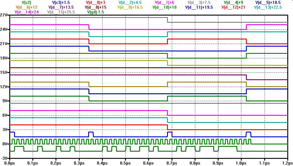
4 short c3 pulses can be seen initializing conversion at 0V level.
Below is c2 clock for acquisition of gd data below.
The correct output data can be seen after 0.35us, 7us and 1.5us.
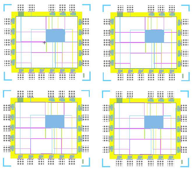
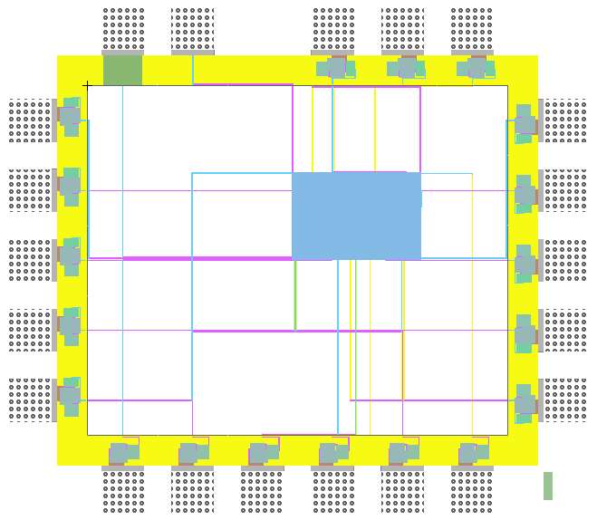
Create a chip adding Pads (, test structures and alignment marks)
Use and load the library Pads4u.jelib.Keep SGrayBinary as the "Current Library".
Create a pad frame placing file (.arr) according to Help.
Search in "Help" - "User's Manual" for 'padframe'.
Copy the example padframe in a file. (.arr)
Modify the file according to the inputs and outputs.
Insert in the line core your top level circuit layout name.
Names are case sensitiv.
Try to make a square pad frame:
Text file: sGrayPad.arr
Tools - Generation - Pad Frame Generator
Tools - Routing - Sea of Gates Route
Remaining steps for production
- Chip identifier name is placed
- Alignment marks are placed
- Multiple chips are placed on one reticle
- Test structures are placed on or between the chips
- Fill structures are placed to generate a regular pattern
- Mask generation is started for each layer
- Layers can be resized for correct pattern transfer
Result
Reticle