Open Laboratory 2022: Adder Investigation
Joerg VollrathLaboratory Instructions
Goal is to verify results of paper [1]
[1] Analysis and Comparison on Full Adder Block in Submicron Technology, M. Alioto; G. Palumbo
[2] Two New Low Power High Performance Full Adders with Minimum Gates
[3] Journal of Computers 2009
and investigate technology changes 1µm..180nm.
Each group takes one architecture, does a layout and simulation with certain technologies and compares results.
Full Adder architecture
Examine Publication [1]Inputs and outputs
| Name | Function | |
| VDD | input | Power |
| A | input | Adder bit A |
| B | input | Adder bit B |
| Ci | input | Carry in bit |
| S | output | Sum bit |
| Co | output | Carry out bit |
| /S | output | Inverted sum bit |
| /Co | output | Inverted carry out bit |
Truth table
S = (A/B/Ci) + (/AB/Ci) + (/A/BCi) + (ABCi)
Co = AB + (A+B)Ci
| A | B | Ci | S | Co |
| 0 | 0 | 0 | 0 | 0 |
| 0 | 0 | 1 | 1 | 0 |
| 0 | 1 | 0 | 1 | 0 |
| 0 | 1 | 1 | 0 | 1 |
| 1 | 0 | 0 | 1 | 0 |
| 1 | 0 | 1 | 0 | 1 |
| 1 | 1 | 0 | 0 | 1 |
| 1 | 1 | 1 | 1 | 1 |
Publication year: [1] 2002 [2] 2009 [3] 2009
Used technology in [1]: 0.35 µm
Minimum size transistors and minimum power delay design.
| Reference | Name | Transistor count | Name |
| [1] | CMOS | 28 | ****35 WN, ****75 SS, ****28 AB, ****23 AS |
| [1] | Mirror | 28 | ****26 ES, ****66 HS, ****78 MB, ****36 RE |
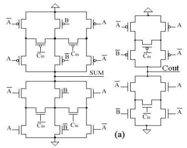
| [1, 2] | CPL | 32 | ****82 DS, ****10 HM, ****42 GJ |
| [1] | LEAP | 22 | ****79 MZ, ****07 BS, ****06 HA, ****76 KR |
| [1] | LP | 16 | ****78 YC, ****95 SR, ****51 PA, ****22 RI |
| [1] | TG | 16 | |
| [1] | TGdrivecap | 26 | ****10 BA, ****23 JF, ****27 ES |
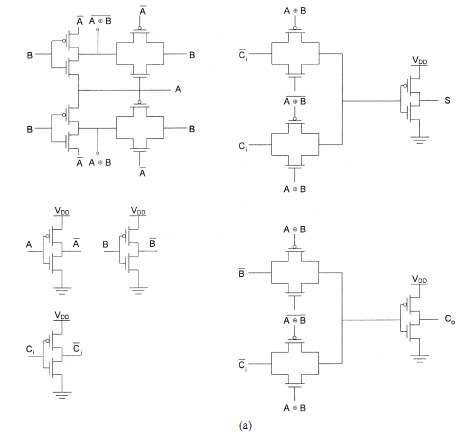
CMOS full adder
Mirror Adder
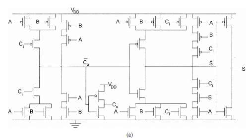
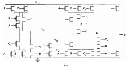
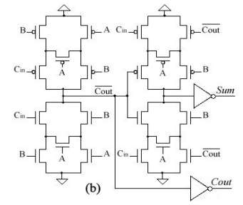
CPL Adder
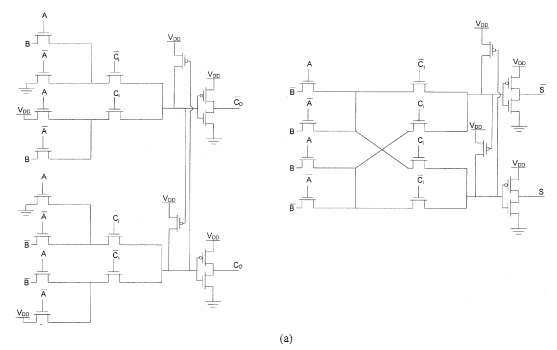
LEAP Adder
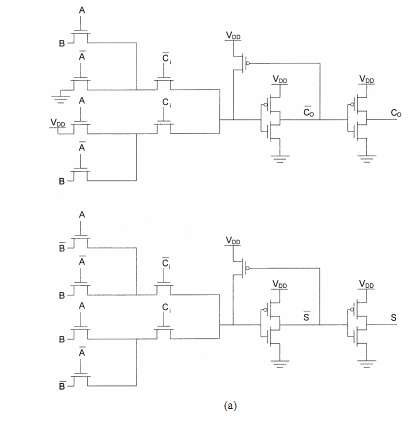
LP Full Adder
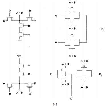
TG Full Adder
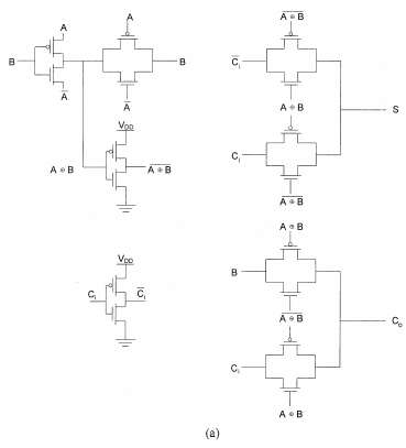
TGdrivecap Full Adder

Tasks
Each group takes one architecture, does a layout and simulation with a certain technology and compares results.
Sources for A, B and Ci are inverters.
Loads for S and Co are inverters.
Compare area per transistor for your design compared to publication.
Make a Table II [1] for your process dimensions, by analyzing a minimum sized inverter simulation for nominal VDD.
Do functional verification (truth table) for each adder at the following supply voltages.
VDD = (Vthn + Vthp) * (1, 1.25, 1.5, 1.75)
Minimum, low voltage, nominal voltage, high voltage
Evaluate power consumption and delay with f=50 MHz
Transistor models
Baker: 1 µm MOSFET model, 50 nm MOSFET model, cmosedu_models.txt
Sedra Smith Level=1 5 µm, 0.5 µm: sedra_lib.lib
Allen, Holberg Level=3 0.8 µm: Holberg.txt
TSMC 0.25um CMOS MOSFETs (level 3) t14y_tsmc_025_level3.lib from MOSIS .
TSMC 0.18um CMOS MOSFETs (level 3) t92y_mm_non_epi_thk_mtl-params_TSMC_018.txt from MOSIS .
Deliverables
1 bit full adder layout and simulation with feature size F1 and F2 at VDD nom, low, high
4 bit adder layout Feature size F and simulation results at VDD nom, low, high
Discussion of your paper (results, presentation) compared to the references.
Maximum 4 pages.
2022_Micro_Adder_<Initials>.jelib
2022_Micro_Adder_<Last name>.pdf
Deadline: 8.07.2022