Specification
|
|
- Input and output signals
Input: CLK, WE, A0, D0..Di, EN Output: PWM - Include a clock generator?
- Make a schematic, layout and simulation
- Extract propagation delay and power consumption
- Make a data sheet
Xilinx Vivado PWM
Start Xilinx Vivado. Configure the project part "xc7a35tcpg236-1" for BASYS3 board and VHDL.
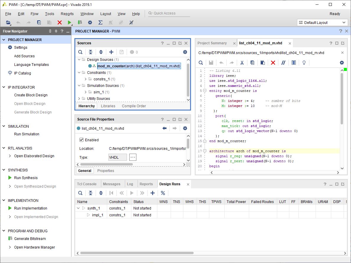
Figure: Vivado project manager
Add list_ch04_11_mod_m.vhd as Design Sources
Add Basys3_Master.xdc as Constraints
Edit constraint file: switches, LED counter selection and setting (upper bits),
PMOD: PWM signal for servo and oscilloscope
Create top level pwm
Create test top level pwm
Create variants
Create synthesis file:
After synthesis run Tcl console write_vhdl <filename>. This gives a structural post synthesis description.
Add Basys3_Master.xdc as Constraints
Add list_ch04_11_mod_m.vhd as counter
Add top_pwm.vhd as top file connecting to hardware
Add top_pwm_sim.vhd for simulation
I0 is mapped to cntUpLUT3:A0i and cmpUpLUT3:B
I1 is mapped to cntUpLUT3:A1i and cmpUpLUT3:A
I2 is mapped to cntUpLUT3:Ci and cmpUpLUT3:lessi
I3 is mapped to cmpUpLUT3:eqi
The sequence is chosen according to the truth table columns
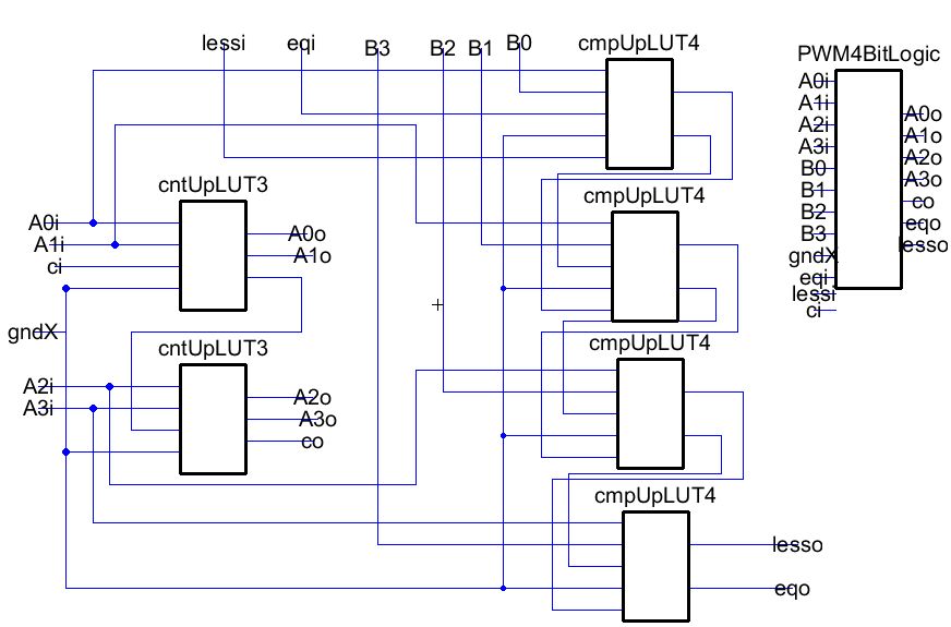
PWM Break down
Blocks:
|
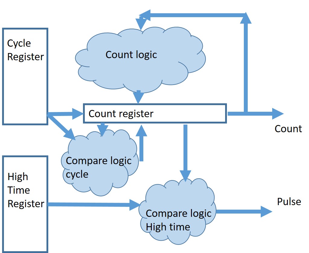 |
PWM Break down
Variations:
|
|
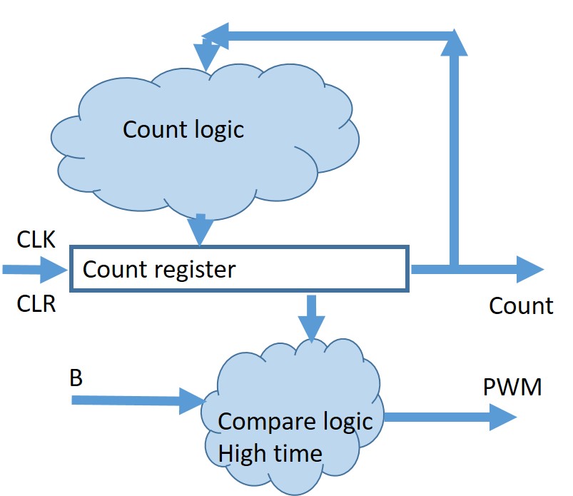
PWM Task Reduction
4 Bit Variations:
|
 |
Count and compare schematic and layout
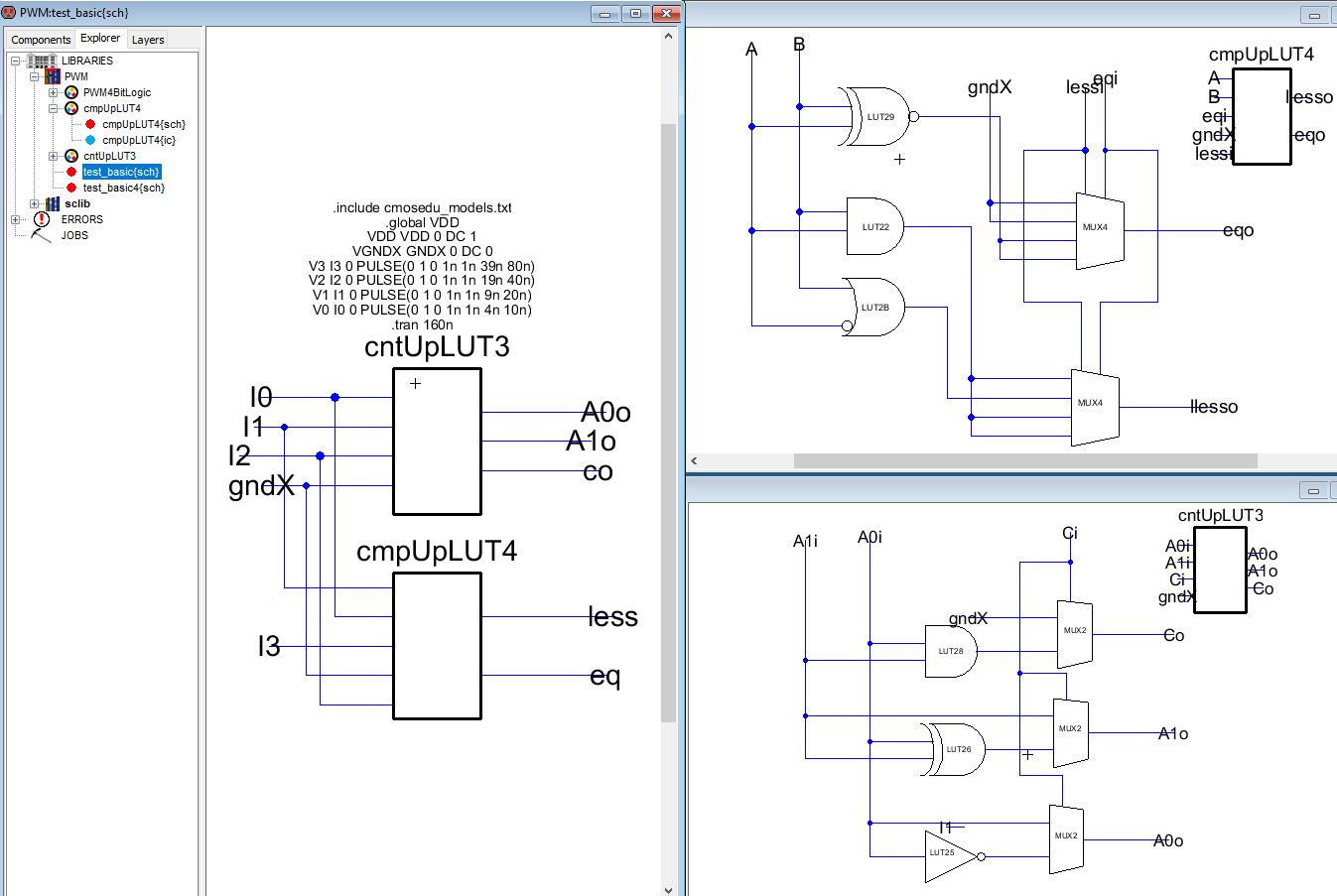
Load sclib
Silicon compiler LUT4_37E5
Do DRC check to make sure that there are no errors
Preferences, Technology, Technology, check Alternative active and poly contact rules
Create new library: PWM
Create cell schematic cntUpLUT3, cmpUpLUT4 and connect
Component, Misc, Library: sclib, MUX2{ic} New Instance
Use extra signal gndX and vddX for 0 and F
Create View Make icon
Create cell schematic test_basic for simulation with cntUpLUT3, cmpUpLUT4
count and compare simulation
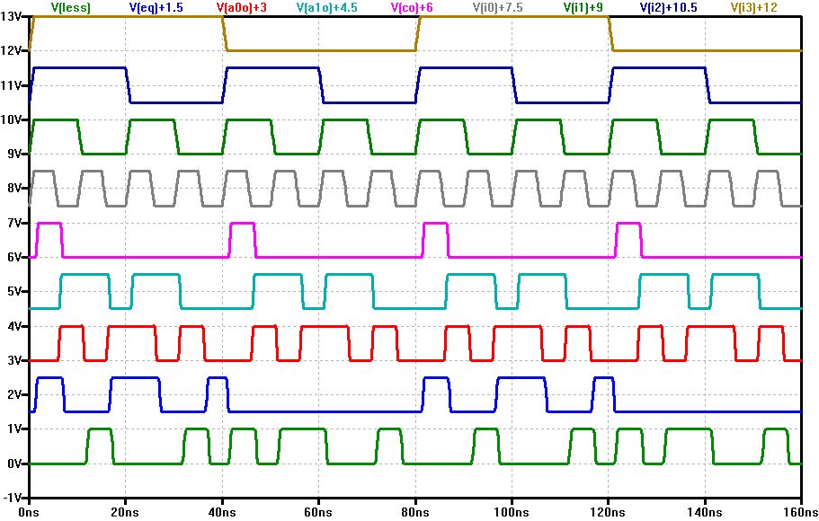
Each column in the simulation of a
combination I0..I3 is one row in the truth table.
The first column from 0..10ns is for the input "1111".
The first column from 0..10ns is for the input "1111".
4 Bit count and compare schematic and layout
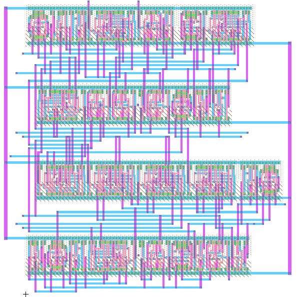
rows length width
4 737 x 747 = 550539
3 921 x 584 = 537864
2 1257 x 462 = 580734
4 737 x 747 = 550539
3 921 x 584 = 537864
2 1257 x 462 = 580734
4 Bit count and compare logic schematic and layout
rows length width
4 737 x 747 = 550539
3 921 x 584 = 537864
2 1257 x 462 = 580734
Bigger tables
4 841 x 857 = 720737
4 737 x 747 = 550539
3 921 x 584 = 537864
2 1257 x 462 = 580734
Bigger tables
4 841 x 857 = 720737
4 Bit count and compare logic simulation
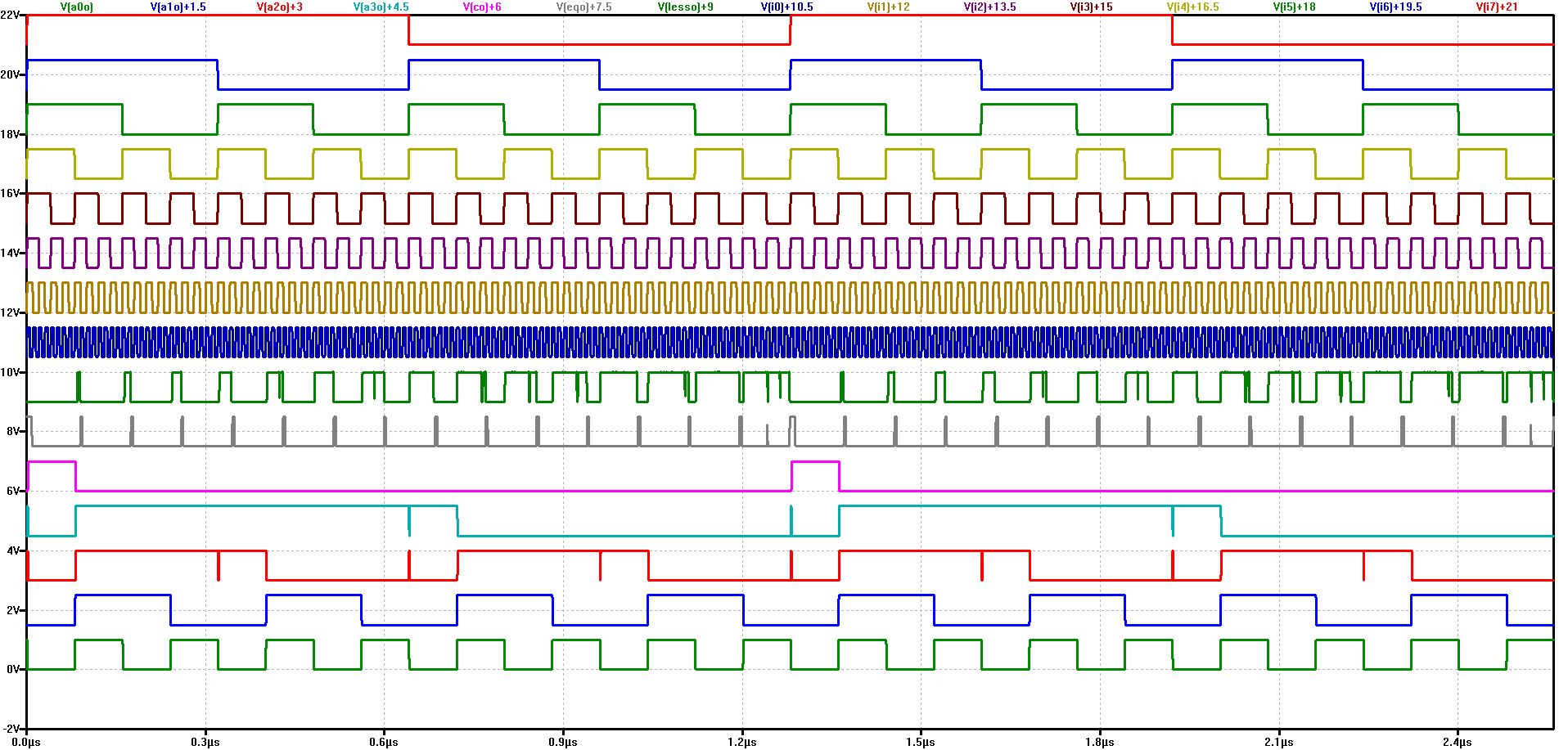
.include cmosedu_models.txt
.global VDD
VDD VDD 0 DC 1
VGNDX GNDX 0 DC 0
VDDX VDDX 0 DC 1
V8 I8 0 PULSE(0 1 0 1n 1n 1279n 2560n)
V7 I7 0 PULSE(0 1 0 1n 1n 639n 1280n)
V6 I6 0 PULSE(0 1 0 1n 1n 319n 640n)
V5 I5 0 PULSE(0 1 0 1n 1n 159n 320n)
V4 I4 0 PULSE(0 1 0 1n 1n 79n 160n)
V3 I3 0 PULSE(0 1 0 1n 1n 39n 80n)
V2 I2 0 PULSE(0 1 0 1n 1n 19n 40n)
V1 I1 0 PULSE(0 1 0 1n 1n 9n 20n)
V0 I0 0 PULSE(0 1 0 1n 1n 4n 10n)
.tran 2560n
The columns are compared with the truth table. The results match. Verification is successful.
Delay
4 Bit PWM schematic
Adding FDC registers for counting and pwm buffer gives 'PWM4Bit'
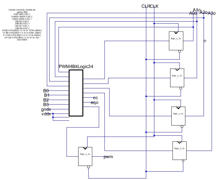
Inputs: CLK, CLR, B3..B0, gndX, vddX
B3..B0 determines the width of the high pulse
Outputs: A3..A0, pwm (lesso), eqo, co
Adding Ci instead of connection to vddX and eqi, lessi instead of connection to vddX would make this module scalable.
B3..B0 determines the width of the high pulse
Outputs: A3..A0, pwm (lesso), eqo, co
Adding Ci instead of connection to vddX and eqi, lessi instead of connection to vddX would make this module scalable.
4 Bit PWM Simulation
The upper trace shows the PWM signal for different setting B0, B2
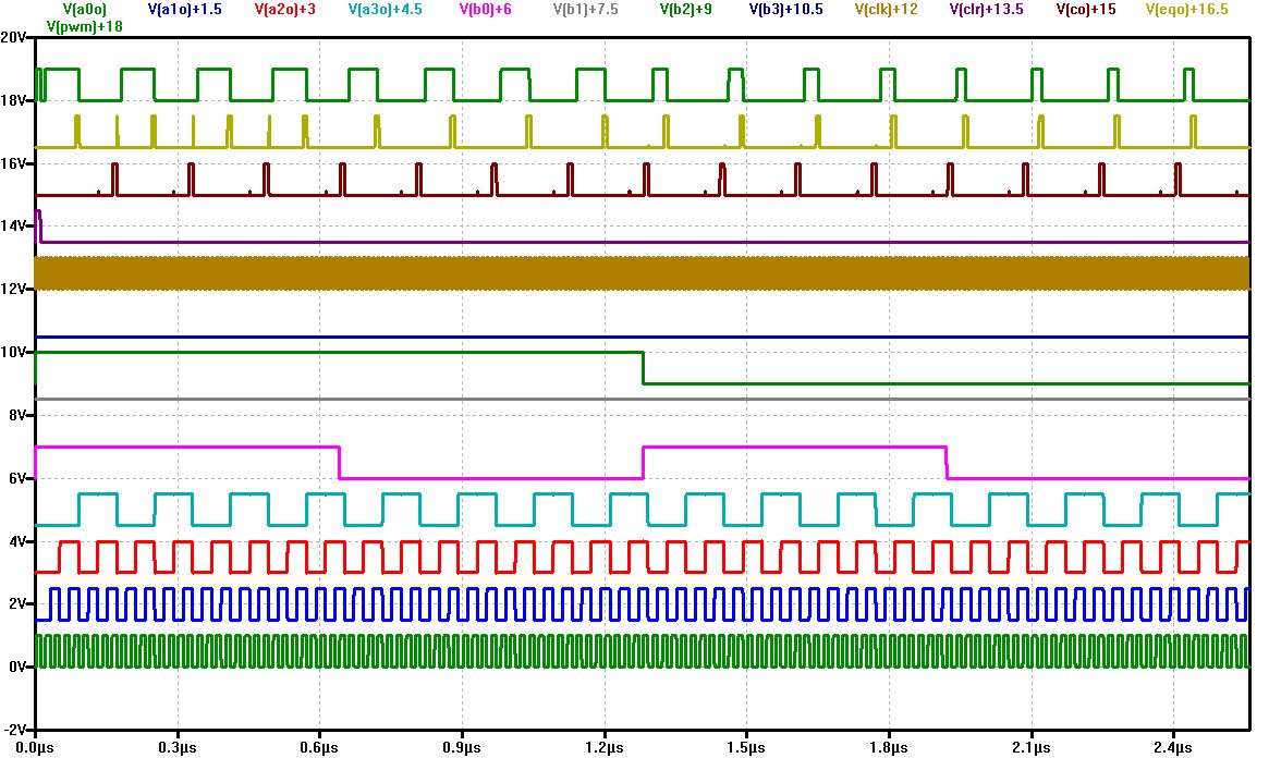
Simulation commands
.include cmosedu_models.txt
.global VDD
VDD VDD 0 DC 1
VGNDX GNDX 0 DC 0
VDDX VDDX 0 DC 1
VB3 B3 0 DC 0
;VB2 B2 0 DC 1
VB1 B1 0 DC 1
;VB0 B0 0 DC 0
V8 B2 0 PULSE(0 1 0 1n 1n 1279n 2560n)
V7 B0 0 PULSE(0 1 0 1n 1n 639n 1280n)
V1 CLR 0 PULSE(0 1 0 1n 1n 9n 2560n)
V0 CLK 0 PULSE(0 1 0 1n 1n 4n 10n)
.tran 2560n
4 Bit PWM layout
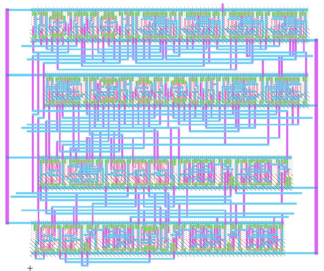
Area rows length width
Area 4 rows 921 x 779 = 717459
Area 5 rows 840 x 921 = 773640
Area 3 rows 1216 x 625 = 760000
Power: VDD, GND, vddX, gndX
Input: CLK, CLR, B3..B0
Output: A3..A0, co, eqo, pwm
Area 4 rows 921 x 779 = 717459
Area 5 rows 840 x 921 = 773640
Area 3 rows 1216 x 625 = 760000
Power: VDD, GND, vddX, gndX
Input: CLK, CLR, B3..B0
Output: A3..A0, co, eqo, pwm
4 Bit PWM layout with Padframe
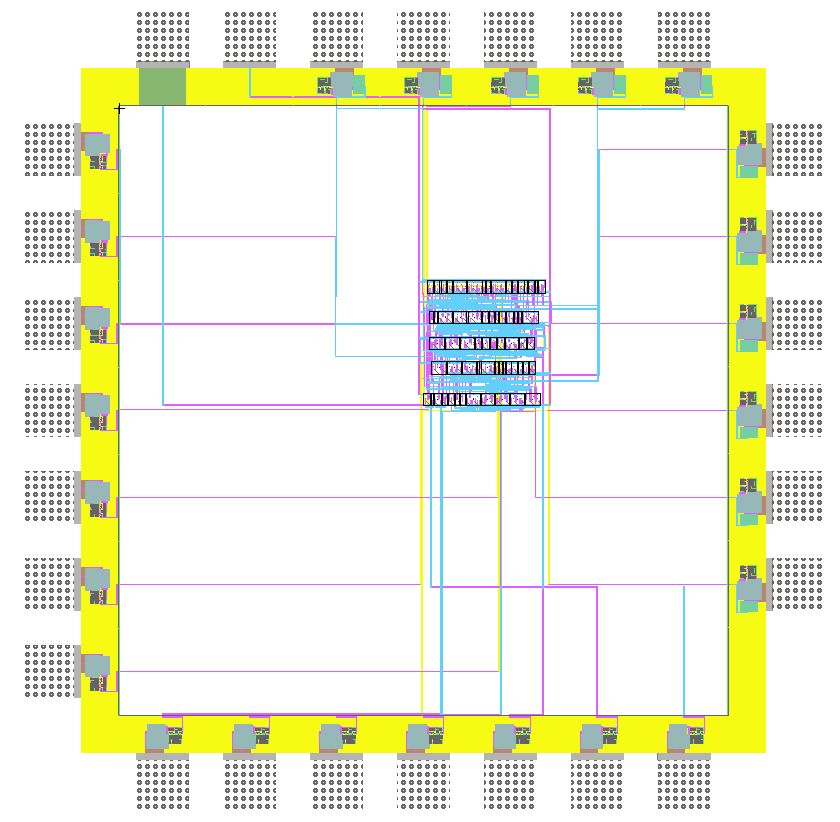
Adding Padframe to serial to gray code converter
Adding Pad Frame
Use and load the library Pads4u.jelib.
Keep multiplier as the "Current Library".
Download file padsMultiplier2x2.arr and save it to your local directory.
Modify the file according to the inputs and outputs.
Insert in the line core your top level circuit layout name.
Names are case sensitiv.
Try to make a square pad frame:
Tools - Generation - Pad Frame Generator: select file padsMultiplier2x2.arr
Tools - Routing - Sea of Gates Route