Hochschule Kempten      
Fakultät Elektrotechnik      
Microelectronics       Fachgebiet Elektronik, Prof. Vollrath      

Microelectronics Laboratory

2024 CMOS Performance

Prof. Dr. Jörg Vollrath


Outline

This laboratory looks at technology scaling, transistor and circuit performance.

A step by step update will be done.

Motivation


  • With technology scaling transistor and circuit performance is changing
  • There are limited examples of SPICE model files available
    Searching for SPICE model 40 nm / 90 nm / 130 nm
  • There are limited performance examples for simulation and measurement of transistors and circuits
  • Rarely transistor curves and parameters are shown with typical ring oscillator and inverter measurements
  • Goal
    • Find transistor IV curves and parameters
    • Do circuit measurement and simulations
    • Look at relationship between technology node and circuit performance
Technology nodes: Wikipedia technologie nodes (02 History Microelectronics)
MOSFET models: 03 MOSFET, Microelectronics

SPICE transistor models


International Electronic Device Meeting IEDM


Performance Circuit: Inverter and Ring Oscillator


  • Inverter
  • Inverter chain
  • Ring oscillator


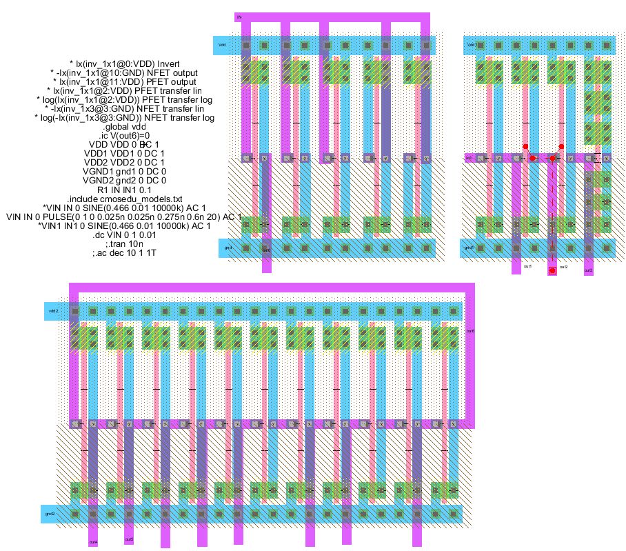
Library: Lab05_2024.jelib


Link: Lab05_2024.jelib

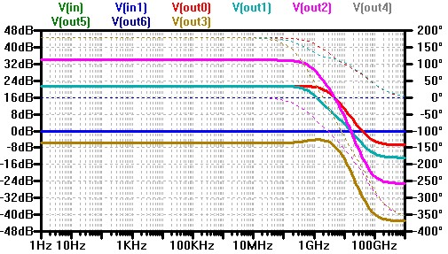
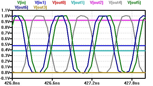
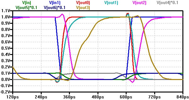
Cell: 'Performance' for .AC and .TRAN ring oscillator and delay simulation
Cell: 'PerformanceDC' for .DC simulation
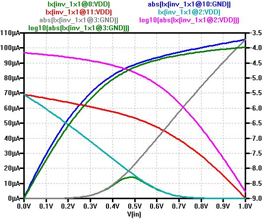
Transistor parameters: Vthn, β (KP,KN), λ
Electrical parameters: VDDmax, (IDSmax), Ioff, Ron, Cox
Performance parameters: tdelay, fCLKmax, gain, ft

Most of the time MOSFETs are not available for measurement, therefore an inverter is used.
The input is fixed at VDD or gnd. With a load NFET or PFET current is measured for the output curve.
The inverter Vout, Iout versus Vin curve gives the threshold voltage Vthn, Vthp and the β (KP, KN).

An Inverter chain gives the propagation delay per stage.
t = 0.7 * R * C
The average power consumption for full charging should be:
Pavg = V * I = V * C * V * f
Changing the load 1,2,3 inverters, changes C while keeping R constant.

DC Simulation Inverter (50nm)


* Ix(inv_1x1@0:VDD) Invert
* -Ix(inv_1x1@10:GND) NFET output
* Ix(inv_1x1@11:VDD) PFET output
* Ix(inv_1x1@2:VDD) PFET transfer lin
* log10(abs(Ix(inv_1x1@2:VDD))) PFET transfer log10
* -Ix(inv_1x1@3:GND) NFET transfer lin
* log10(abs(Ix(inv_1x1@3:GND))) NFET transfer log10
.option TEMP = 27
VIN IN 0 SINE(0.466 0.01 10000k) AC 1
.dc VIN 0 1 0.01
Vth, β λ; Imax, Ioff

Trace:
Ix(inv_1x1@0:VDD) -Ix(inv_1x1@10:GND) Ix(inv_1x1@11:VDD) Ix(inv_1x1@2:VDD) log10(Ix(inv_1x1@2:VDD)) -Ix(inv_1x3@3:GND) log10(-Ix(inv_1x3@3:GND)) NFET transfer log
λ is valid for the linear part of the output curve IDS(VDS) where VGS-Vth < VDS
One point is maximum VDD, IDS and the other is less VDS where IDS(VDS) is still linear.
λ = (IDS1 - IDS2)/(IDS2 * UDS1 - IDS1 * UDS2)
NFET: λn = (105uA-100uA) /(100uA * 1V - 105uA * 0.8V) = 5uA/(16uaV) = 0.3 V-1
PFET: λp = (69uA-61uA) /(69uA * 1V - 61uA * 0.7V) = 8uA/(27uaV) = 0.3 V-1

KNn = 2 * IDSmax * L / W / (1+ λ VDS) / (VGS -Vth)^2
NFET: KNn = 2 * 105 uA / 3.5 / (1+ 0.3) / (1 V - 0.25)^2 = 82 uAV-2
PFET: KNn = 2 * 69 uA / 5 / (1+ 0.3) / (1 V - 0.25)^2 = 38 uAV-2

RDS = W/L * (VDD-V(IDSmax/2))/(IDSmax - IDSmax/2)
RDSn = 3.5 * 0.35 V / 51 uA = 20 kΩ
RDSp = 5 * 0.35V / 35 uA = 50 kΩ

Gain:
Look at IDS at voltage VDD/2 for gain calculation.
\( v_u = \frac{dVout}{dVin} = \frac{1}{ I_{DS}(V_{DD}/2) \cdot λ \cdot RDS} \)
\( R_{DS} = \frac{1}{\frac{1}{R_{DSn}} + \frac{1}{R_{DSp}}} = 14 k\Omega \)
\( v_u = \frac{1}{15 uA \cdot 0.3 V^{-1} \cdot 14 k\Omega} = 24 \)
avu = 21 dB
Are there better equations for simple calculation of parameters?
What would be the optimum WN/WP ratio?
What is the effect of changing L?
What happens if LN/LP is not 1?

AC Simulation Inverter (50nm)


VIN IN 0 SINE(0.466 0.01 10000k) AC 1
.ac dec 10 1 1T
V(out0): output inverter, no load
ft 40GHz, a = 22dB
V(out1): load inverter
ft 16.8 GHz, a = 22 dB

A operation point of 0.466 V is set to be at the maximum gain point of the inverter.

Definition of transit frequency ft(a = 0 dB)
ft = gm/2/pi/CGD = 1/RDS/2/pi/CGD
Estimation of Area for CGD:
W * L no load = 8.5; W * L inverter load = 2.5 * 8.5 = 21
Cox = 8.5 CGD
Cox = 1/(W * L * ft * RDS * 2 * pi) = 1/(8.5 * 40 GHz * 14 kΩ * 2 * 3.14) = 33 aF

How is a and ft changing with temperature?
How is a and ft changing with voltage (Offset/bias and VDD)?
.step TEMP LIST -10 27 90
.step VDD1 0.9 1.1 0.1 

Delay Simulation Inverter and Ring Oscillator (50nm)


Ring oscillator:
Cycle time 650 ps
11 stages (60ps per stage)

VIN IN 0 PULSE(0 1 0 0.025n 0.025n 0.275n 0.6n 20) AC 1
.tran 10n

Delay:
Nominal 1x: 2.5 Cox HL: 22 ps, LH: 28 ps;
Load 3x: 5.5 Cox 32ps, 46 ps
Delay is measured from V(out1) to V(out2) (no load) and from V(out2) to V(out3) (with load) for rising and falling edges.

Performance Table

NameNominalChange Change F
Feature size50 nm (Baker)VDD max1 V
T27 °CImaxInv15 uA
Ln50 nmLp50 nm
Wn175 nmWp250 nm
IDSn max105 uAIDSp max70 uA
Vthn0.25 VVthp-0.25 V
KNn82uAV-2KNp38uAV-2
λn0.3 V-1λp0.3 V-1
Ioffn1E-9 AIoffp2E-9 A
Coxn33 aFCoxp33 aF
RDSn20 kΩRDSp50 kΩ
gain22 dB, 100tRing11650 ps
ftmax40 GHzftreal16 GHz
tpdHLx122 pstpdLHx128 ps
tpdHLx332 pstpdLHx346 ps

Column Change can be:

Deliverables


Future work and questions