Microelectronics03 MOSFETProf. Dr. J—rg Vollrath02 History |

|
Video of lecture 03 MOSFET, SPICE models, propagation delay 31.03.2021
|
Lðnge: 01:26:05 |
0:0:0 0 0:3:9 Goals today 0:6:36 Output and transfer curve 0:9:48 50 nm technology voltage limit 0:14:58 Subthreshold characteristic 0:16:49 Bulk source voltage and threshold voltage 0:19:25 Design by selecting W or number of unit transistors 0:24:29 MOSFET typical layout and rules 0:30:37 SPICE models 1 um, 50 nm 0:35:39 Infineon 130 nm MOSFET transistor parameters 0:40:29 SPICE models details 0:48:31 MOSFET as switch 0:50:39 Transistor RC model 0:52:39 Transistor Capacitances 0:59:19 Propagation delay 1:1:39 Rising and falling output 1:8:49 equivalent capacitance, Miller capacitance 1:16:49 Timing closure |
Microelectronic products
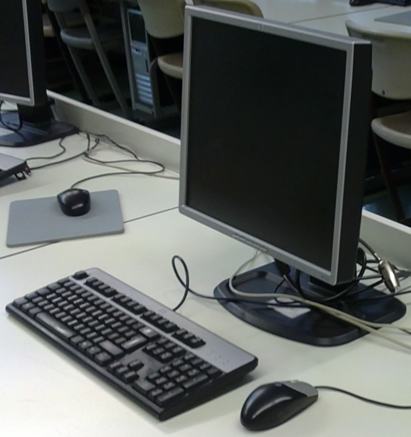 Computer |
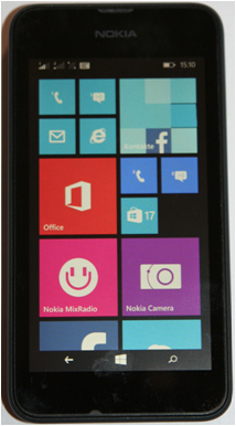 mobile phone | ||||
Consumer |
Automotive |
Industrial | |||
Hierarchical Description
| Top Down | System Subsystemi, Subsystemj Subsystemk, Subsysteml |
Bottom up |
Find one solution and then optimize
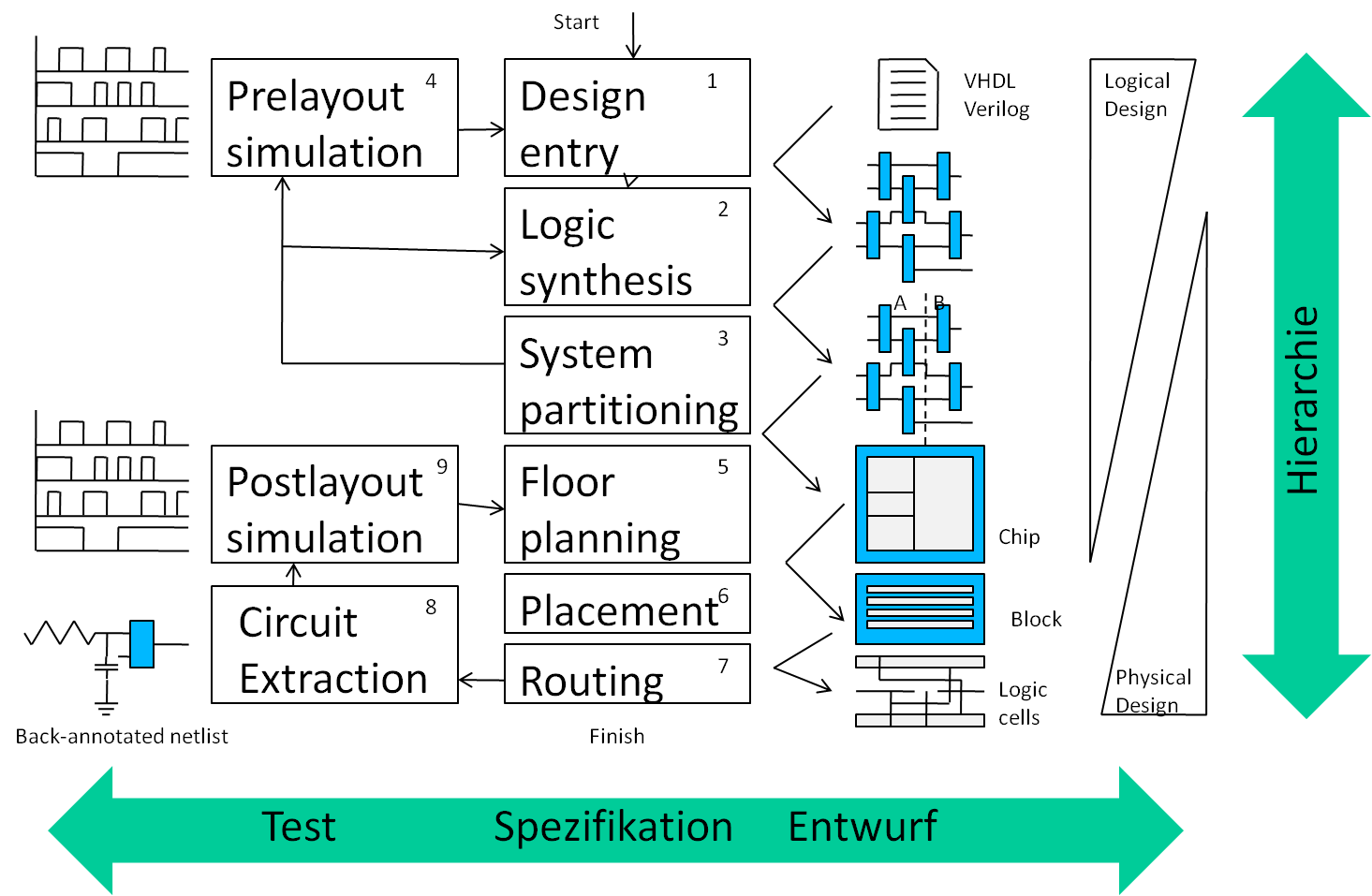
Design Flow
Technologies
| Comparison |

ASIC |

FPGA |

Microcontroller |
| Target market | High volume | Prototype to medium volume | Single to high volume |
| Design speed | Slow | Fast | Faster |
| Design Tools | Expensive | No cost | No cost |
| Efficiency | Optimum | slow clock, parallel operation | slow clock, seriell operation, analog function |
ASIC: Application specific integrated circuit.
FPGA: File programmable gate array.
FPGA: File programmable gate array.
Systems (1)
Raspberry Pi: µC, peripheryOperating system: LinuxCommunication: Wifi, Webserver C(++), JavaScript Application: C(++), JavaScript |
.jpg)
|
Arduino: Microcontroller (µC)No operating systemApplication and Communication C |
Matlab, Labview can support some platforms.
Systems (2)
Zedboard: FPGA, µCField programmable gate array (FPGA)FPGA programming: VHDL, Verilog, IP Wizard Optional operating system: Linux Communication: Wifi, Webserver C(++), JavaScript Application: C(++), JavaScript |
 Switch matrix, logic and registers, programmable |
ASICProprietory software for design Electronic design automation (EDA) software tools: linux, perl, phyton, JavaScript |
Full custom ASIC Standard cell ASIC Gate Array Based Asic Foundries: TSMC, UMC Educational: MOSIS Europractice Zero To ASIC |
Matlab, Labview can support some platforms.
Electronic system

System Description
Modelling Simulation Structural Description Behavioral Description |
Analog and digital signals
|
Transistor Evolution
|
How much area uses one transistor? Theoretical minimum: Active area: W*L*4 Contacts: W*L*4*3 Minimum Feature size F A=16*F2 Example: F = 45 nm; 731M Transistors; 262 mm2 A = 262 mm2/(731*106)= 358413 nm2 = 177*F2 |

|
 Courtesy of Intel 2008 Intel Core i7 731 Million MOS Transistors 45 nm process 263 mm2 2.6..3.2 GHz |
Summary Transistor Evolution
MOSFET- transistorMoores law
Implications of reduced feature size:
30% Productivity gain per year
Power consumption, complexity/features, price
Hierarchical Design
Verification
Microelectronics deals with small electronic components
Transistor, diode, resistor, capacitor, inductance
Microelectronic systems are getting cheaper
Complex systems can be realized
Functions are getting cheaper
Typical microelectronic components of interest are:
Microcontroller (Microprocessor, memory, digital and analog functions)
FPGA (Field programmable gate arrays)
ASIC (Application specific integrated circuits)
This class shows how to design digital and analog CMOS microelectronic components and systems
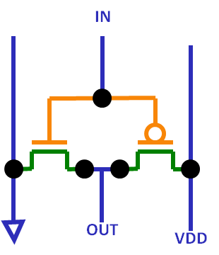
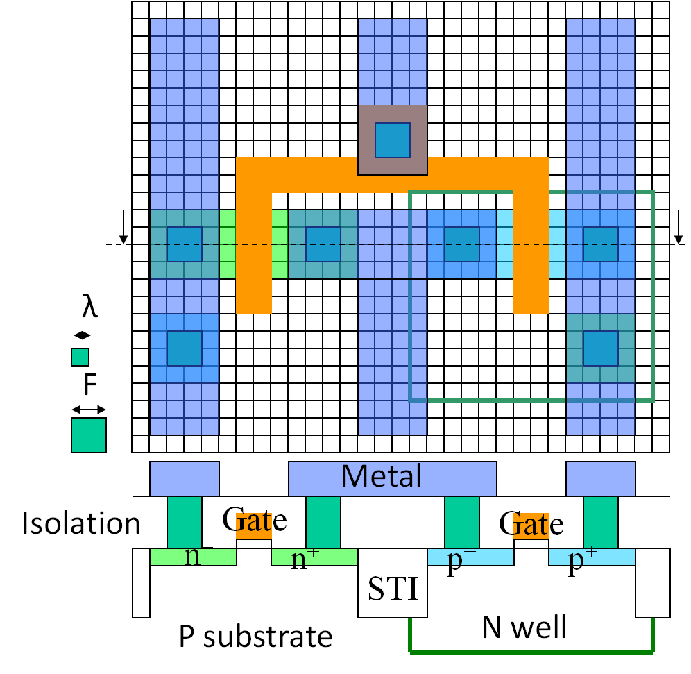
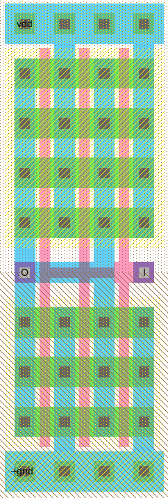
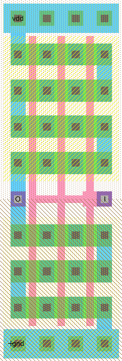
Inverter schematic and layout
|
|
Schematic and layout are representing an inverter.
An inverter uses a NMOSFET and a PMOSFET.
The schematic shows the components and connections.
The layout has added different colors for different layers of the manufacturing process and each component.
These colors are transferred into the schematic showing the relationship between layout and schematic.
Wiring and transistor gates and diffusion have a minimum physical size of width and length of F.
There are also minimum distances required to prevent shorts.
It is difficult to automatically transform one view into the other.
A schematic is drawn to be able to easily understand the circuit. On the left is GND, on the right VDD, on the top inputs, on the bottom outputs.
In a schematic connection between 2 pins can be accomplished by labeling the pins with the same names. Lines can cross without resulting in short circuits.
A layout is drawn for symmetric and regular patterns, avoiding signal cross coupling and shape distortion, and having minimum size.
Equations of a n-channel MOSFET
|
\( I_{DS}= \cases{
\begin{matrix}
0 & \text{for} & V_{GS} \leq V_{th} & \text{Off}
\\
I_{on} exp^{\frac{ V_{GS}-V_{th} - \frac{kT}{e}}{\frac{kT}{e}}} \left( 1+\lambda V_{DS} \right)
& \text{for} & 0 \leq V_{GS} - V_{th} \lt \frac{kT}{e} & \text{Weak inversion}
\\
\beta \left( V_{GS}-V_{th} \right)^2 \left( 1+\lambda V_{DS} \right)
& \text{f■r} & \frac{kT}{e} \leq V_{GS} - V_{th} \lt V_{DS} & \text{Saturation}
\\
\beta \left( 2 \left( V_{GS}-V_{th} \right) V_{DS} - V_{DS}^2 \right)
& \text{for} & \frac{kT}{e} \leq V_{GS} - V_{th} \geq V_{DS} & \text{Linear}
\end{matrix}
}
\) \( \beta = \frac{\mu_n \epsilon_{ox}}{2d_{ox}} \frac{W}{L} = \frac{1}{2} \mu_n C_{ox}^{'} \frac{W}{L} = \frac{1}{2} K_{n}^{'} \frac{W}{L} = \frac{1}{2} K_{n} \) |
 Quelle Vollrath
 |
 Quelle Vollrath
 |
Draw a IDS(VGS) and IDS(VDS) curve with Vth = 1V (0.3V), Kn = 100 µAV-2 and λ = 0.02 V-1
Vth threshold voltage
λ Output conductance
W width, L length
µ mobility
Cox = e /dox Gate oxide capacitance
Vt = kT/q (300K) = 0.0259 V
Simulation verifies first correct Vth and maximum current IDS at maximum voltage Vdd.
Then the input capacitance Cox is confirmed with AC simulation of a RC circuit having the MOSFET gate as capacitance C.
Microelectronic has only transistors as elements.
Design is done using transistors with choosing W and L.
MOS transistors are also used as capacitances, resistors, diodes and lateral bipolar transistors.
In sub 50nm processes FINFETs are used having a fixed L and W. These transistors are called unit transistors. Circuits are designed combining transistors in series or parallel to get the desired W/L ratio. This makes automated design easier.
Elektronik 3, 08 MOSFET
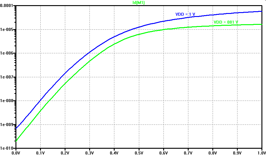
NFET Transistor subthreshold characteristic
|
MOSFET transistors can also be operated in the subthreshold region for low voltage power supply.
The graph shows an increase in current by a factor of 10 for 100 mV change in VGS.
MOSFET layout
|
|
|
sclib.jelib: UNITExample{lay}, UNITLong{lay}
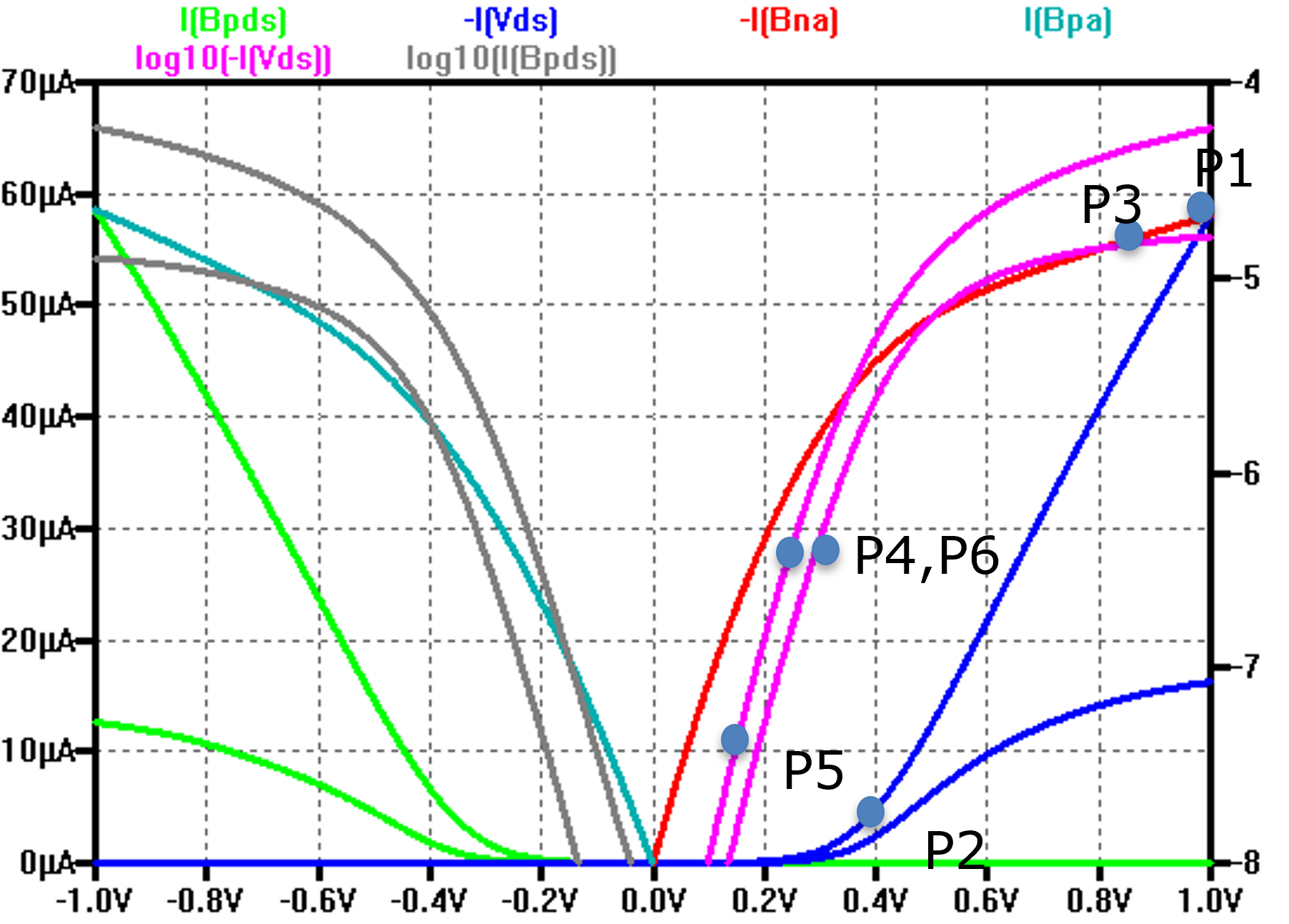
Detailed Transistor measurement
|
VDD LN=LP=F, WN = 2F, WP = 4F P1: Ion = IDSmax P1, P2: Vth, Rdson (KP) P1, P3: λ P4, P5: SS(mV/dec), Ioff P4, P6: DIBL(mV/V) |
|
The graph combines PFET and NFET characteristic in linear and logarithmic y scale.
Minimum dimensions are used as stated above.
Transistor parameters can be extracted using the points P1..P6.
For subthreshold slope (SS), drain induced barrier lowering (DIBL) and Ioff the logarithmic curves are analyzed. Logarithmic behaviour can be seen starting below Vth/2.
Ix = Ids(Vgs=Vthn*0.5/Vthp*0.7)
SS = V(Ix) - V(Ix/10)
DIBL = (V(Ix;VDSmin) - V(Ix;0.1*VDSmax))/0.9/VDSmax
Ioff = Ix * 10^(-Vth/2/SS)
An example simulation with measurement statements for 50nm technology (Baker) is given in CMOS_IV_50n.spi
| NFET | L=F, WN=2F | L=F, WN=4F | L=2F, WN=4F |
| inmax = inon | 58uA | 121uA | 44uA |
| vtn | 0.35V | 0.35V | 0.39V |
| rnon | 11kOhm | 5.4kOhm | 13.8kOhm |
| lambdan | 0.308/V | 0.308/V | 0.231/V |
| ssn | 86mV/dec | 86mV/dec | 87mV/dec |
| DIBLn | 37mV/V | 37mV/V | 27mV/V |
| ioffn | 713pA | 1.5nA | 234pA |
| PFET | L=F, WP=4F | L=F, WP=8F | L=2F, WP=8F |
| Ipmax = Ipon | 53.6uA | 115uA | 38uA |
| Vtp | -0.25V | -0.25V | -0.29V |
| rpon | 14kOhm | 6.5kOhm | 18kOhm |
| lambdap | 0.437/V | 0.428/V | 0.242/V |
| ssp | 248mV/dec | 253mV/dec | 279mV/dec |
| DIBLp | 68mV/V | 79mV/V | 29mV/V |
| ipoff | 20.5nA | 44nA | 9.7nA |
130 nm Infineon MOSFET transistors
Infineon 130 nm platform