Microelectronics Laboratory2026 FPU InvestigationProf. Dr. J÷rg Vollrath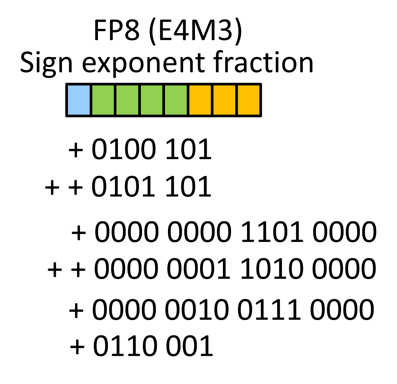 |
Video Microelectronics Laboratory
Video 08.06.2026
|
Duration: 1:08:59 |
0:0:30 Laboratory FPU MIcro 0:1:31 Motivation 0:3:31 Minifloat 0:5:30 Operations 0:9:0 Full Adder Truth Table 0:11:25 Objective 0:11:37 0:11:37 4-Bit Truth Table 0:12:28 Tool for synthesis 0:13:41 Generate Truth table 0:15:21 Structural VHDL 0:18:38 Start VLSI Design System 0:19:23 Download sclib.jelib, pads4u.jelib, padsMulitplier2x2.arr 0:21:50 Open libraries 0:22:30 New library 0:23:5 New cell VHDL 0:24:33 Insert VHDL code 0:25:25 Module name 0:26:25 Generate truth code and copy to VLSI Design system 0:28:10 Exception 0:28:40 Change output names 0:29:5 Error Investigation 0:29:5 Silicon Compiler start with entity 0:30:5 Preferences Tools Silicon Compiler Number of rows 1 0:31:32 Layout 0:31:35 Errors and Fix 0:35:10 0 0:35:10 Simulation of Layout 0:35:35 Manipulate Exports 0:36:45 Get SPICE code 0:39:45 Input Stimulus 0:40:30 Test vector creation HTML 0:42:38 Timing diagram 0:44:10 Copy LTspice simulation code 0:46:1 Simulate LTspice 0:47:5 Number of transistors per subcircuit 0:48:40 Run LTspice look at traces 0:50:50 Timing Propagation Delay 0:53:25 Propagation Delay 0:54:25 Optimization LTSPICE 0:56:45 Simulation 0:57:20 Optimization VHDL 0:58:55 Total size of logic 1:1:15 Pad Frame start 1:2:15 Open .arr file 1:3:25 core name 1:4:15 Change names of signals of Pads 1:5:55 Tools Generation Pad frame 1:7:35 Tools Routing Sea of gates raute 1:7:55 Move core cell to left 1:8:59 Motivation |
Outline
- Motivation and Objectives
- Number formats and operations
Posive integer, negative, fixed point, floating point - Implementations
Full adder, multiplier - Tasks
Truth table application - Deliverables
AI, NPU calculations use floating point numbers
Numbers and Number Formats
- Signed Integer: Sign, complement
8 Bit: +127,0,-128 - Floating point: signed mantisse + exponent 8 Bit FP8 (E3M4): 1 Bit Sign, 4 bit significant, 3 Bit exponent
- Programming, calculation: NaN, +inf, -inf
- Posit8, Talkum8, Posits
- Base for exponent, mantissa: 2,3,4,5,8,(16,32)
- Operations and size of truth table:
- Mapping decimal and number (Truth table size: 2^N)
- Minus -x, Max/x (Truth table size: 2^N)
- Add, multiply, power (Truth table size: 2^(2N))
- Notation: FPn EeMm (1.e.m) n = 1 + e + m
Sign 1, exponent e, mantissa m
FP8-E4M3 (1.4.3)
Sign Exponent Significand
MantisseS E E E E M M M 0 1 0 0 1 0 1 1 1.4.3
Minifloat
3-bit (1.1.1) |
4-bit (1.2.1) | ||||||||||||||||||||||||||||||||||||||||||
|
| ||||||||||||||||||||||||||||||||||||||||||
|
| ||||||||||||||||||||||||||||||||||||||||||
Machine learning
Nvidia "fp8" format (1.5.2, E5M2)
Nvidia: FP8-E4M3 (1.4.3)
FP4-E2M1 (1.2.1)
Operations
Size of truth table:
- Mapping decimal and number (Truth table size: 2^N)
- Minus -x, Max/x (Truth table size: 2^N)
- Add, multiply, power (Truth table size: 2^(2N))
Truth Table Operations 4-Bit
- Minus -x, Max/x
16 codes - Add, multiply, power
256 codes - Operation with NaN gives NaN
- Division with 0 gives +- infinity
- Division with infinity gives 0 or delta
Floating point calculation
Add, subtractConvert to fixed point (shift).Add/subtract(add invert and cin="1"). Convert to floating point (shift). MultiplyAdd exponentMultiply mantissa. Adjust exponent (add) and shift mantissa. DivisionMultiply with max/x. |
Add: SEEM +010 : 1 ++001 : 0.5 ---Fixed point-------- +01.0 : 1.0 ++00.1 : 0.5 ---Add---------------- +01.1 : 1.5 -- Floating point ---- SEEM +011 : 1.5 | ||||||||
FPU Intel 8087 8-Bit
addition, subtraction, multiplication, divison, square root
exponential, logarithmic, trigonometric
50,000FLOPs
100..1000 cycles
65k transitors
CORDIC algorithm
Multi cycle serialization
Scalability for number of bits and time (pipeline possibility)
Arithmetic truth table implementation
Example full adder3 Inputs: a,b,cin 2 outputs: s,cout Standard cell: 28 Transistors per Bit LUT/MUX: 2 * 24 transistors = 48 transistors LUT2, MUX: 30 Transistors per Adder Bit |
|
s = LUT3_69 = MUX2(LUT2_6,LUT2_9) = MUX2(NOT(LUT2_9),LUT2_9 ): 12 transistors
cout = LUT3_87 = MUX2(LUT2_8, LUT2_E) = MUX2(NOT(NAND(I0,I1)),NOT(NOR(I0,I1))): 18 transistors
Sum: 30 transistors
Truth table implementation
How many LUT2s and MUX2, MUX4 are needed for realization of a truth table?
| Number of inputs | Size of truth table | LUT2 | INV | MUX2 | Depth | Total Transistors |
| Number of transistors | 36 | 2 | 4 | 12 | Total Transistors | |
| 2 | 2^2=4 | 1 | 0 | 0 | 0 | 12 |
| 3 | 2^3=8 | 2 | 1 | 1 | 1 | 24 |
| 4 | 2^4=16 | 4 | 2 | 3 | 2 | 34 |
| 5 | 2^5=32 | 8 | 3 | 7 | 3 | 70 |
| 6 | 2^6=64 | 16 | 4 | 15 | 4 | 104 |
| 7 | 2^7=128 | 16 | 5 | 31 | 5 | 170 |
| 8 | 2^8=256 | 16 | 6 | 63 | 6 | 300 |
(2026 Objective)
How many transistors are needed for a typical truth table?
4-Bit Floating point number: Size of truth table is 16
4-Bit Division max/x: Size of truth table is 16
Addder: Size of truth table is 256
Multiply: Size of truth table is 256
Implement 3 truth tables size 16 with LUTs and Verilog.
Make layout and simulate with LTSPICE.
(Expand to larger truth tables)
2026 Objective
Guided implementation of a truth table (max/x) using LUT2 and MUX2
LTSPICE simulation, verification and transistor count
Pad implementation with simulation
Implementation of a larger truth table
LTSPICE simulation, verification and transistor count
4-Bit Truth table Division
| Map0 | Divide | 0 | 1 | 2 | 3 | 4 | 5 | 6 | 7 | 8 | 9 | 10 | 11 | 12 | 13 | 14 | 15 | Student | |
| Original | Code | 0 | 0.25 | 0.5 | 0.75 | 1 | 2 | 3 | +inf | NaN | -0.25 | -0.5 | -0.75 | -1 | -2 | -3 | -inf | ||
| Max/x | Code | +inf | 3 | 2 | 1 | 1 | 0.5 | 0.25 | 0 | NaN | -3 | -2 | -1 | -1 | -0.5 | -0.25 | 0 |
4-Bit Truth table Addder
| Map 0 | 0 | 1 | 2 | 3 | 4 | 5 | 6 | 7 | 8 | 9 | 10 | 11 | 12 | 13 | 14 | 15 | |||
| Add | 0 | 0.25 | 0.5 | 0.75 | 1 | 2 | 3 | +inf | NaN | -0.25 | -0.5 | -0.75 | -1 | -2 | -3 | -inf | Student | ||
| 0 | 0 | 0 | 0.25 | 0.5 | 0.75 | 1 | 2 | 3 | +inf | NaN | -0.25 | -0.5 | -0.75 | -1 | -2 | -3 | -inf | xxxx | |
| 1 | 0.25 | 0.25 | 0.5 | 0.75 | 1 | 1 | 2 | 3 | +inf | NaN | 0 | -0.25 | -0.5 | -0.75 | -2 | -3 | -inf | ******80 ZJ | ******39 PS |
| 2 | 0.5 | 0.5 | 0.75 | 1 | 1 | 2 | 3 | +inf | +inf | NaN | 0.25 | 0 | -0.25 | -0.5 | -2 | -3 | -inf | ******98 DG | ******20 DI |
| 3 | 0.75 | 0.75 | 1 | 1 | 2 | 2 | 3 | +inf | +inf | NaN | 0.5 | 0.25 | 0 | -0.25 | -0.5 | -2 | -inf | ******13 GA | ******33 TG |
| 4 | 1 | 1 | 1 | 2 | 2 | 2 | 3 | +inf | +inf | NaN | 0.75 | 0.5 | 0.25 | 0 | -1 | -2 | -inf | ******26 SS | *******28 MH |
| 5 | 2 | 2 | 2 | 3 | 3 | 3 | +inf | +inf | +inf | NaN | 2 | 2 | 1 | 1 | 0 | -1 | -inf | ******08 LK | |
| 6 | 3 | 3 | 3 | +inf | +inf | +inf | +inf | +inf | +inf | NaN | 3 | 3 | 2 | 2 | 1 | 0 | -inf | ******22 LG | *******08 KV |
| 7 | +inf | +inf | +inf | +inf | +inf | +inf | +inf | +inf | +inf | NaN | +inf | +inf | +inf | +inf | +inf | +inf | 0 | ******86 MN | |
| 8 | NaN | NaN | NaN | NaN | NaN | NaN | NaN | NaN | NaN | NaN | NaN | NaN | NaN | NaN | NaN | NaN | NaN | xxxx | xxxx |
| 9 | -0.25 | -0.25 | 0 | 0.25 | 0.5 | 0.75 | 2 | 3 | +inf | NaN | -0.5 | -0.75 | -1 | -1 | -2 | -3 | -inf | ******80 GD | ******02 RM |
| 10 | -0.5 | -0.5 | -0.25 | 0 | 0.25 | 0.5 | 2 | 3 | +inf | NaN | -0.75 | -1 | -1 | -2 | -3 | -inf | -inf | ******62 PV | ******36 SS |
| 11 | -0.75 | -0.75 | -0.5 | -0.25 | 0 | 0.25 | 1 | 2 | +inf | NaN | -1 | -1 | -2 | -2 | -3 | -inf | -inf | *******38 LR | ******08 SB |
| 12 | -1 | -1 | -0.75 | -0.5 | -0.25 | 0 | 1 | 2 | +inf | NaN | -1 | -2 | -2 | -2 | -3 | -inf | -inf | *******96 JA | xxxx |
| 13 | -2 | -2 | -2 | -2 | -0.5 | -1 | 0 | 1 | +inf | NaN | -2 | -3 | -3 | -3 | -inf | -inf | -inf | *******11 SH | xxxx |
| 14 | -3 | -3 | -3 | -3 | -2 | -2 | -1 | 0 | +inf | NaN | -3 | -inf | -inf | -inf | -inf | -inf | -inf | *******28 IA | xxxx |
| 15 | -inf | -inf | -inf | -inf | -inf | -inf | -inf | -inf | 0 | NaN | -inf | -inf | -inf | -inf | -inf | -inf | -inf | xxxx | |
4-Bit Truth table Multiply
| Map 0 | 0 | 1 | 2 | 3 | 4 | 5 | 6 | 7 | 8 | 9 | 10 | 11 | 12 | 13 | 14 | 15 | |||
| Mul | 0 | 0.25 | 0.5 | 0.75 | 1 | 2 | 3 | +inf | NaN | -0.25 | -0.5 | -0.75 | -1 | -2 | -3 | -inf | Student | ||
| 0 | 0 | 0 | 0 | 0 | 0 | 0 | 0 | 0 | 1 | NaN | 0 | 0 | 0 | 0 | 0 | 0 | -1 | xxxx | |
| 1 | 0.25 | 0 | 0 | 0 | 0.25 | 0.25 | 0.5 | 0.75 | +inf | NaN | 0 | 0 | -0.25 | -0.25 | -0.5 | -0.75 | -inf | ******11 BA | |
| 2 | 0.5 | 0 | 0 | 0.25 | 0.5 | 0.5 | 1 | 2 | +inf | NaN | 0 | -0.25 | -0.5 | -0.5 | -1 | -2 | -inf | ******60 SS | |
| 3 | 0.75 | 0 | 0.25 | 0.5 | 0.5 | 0.75 | 2 | 2 | +inf | NaN | -0.25 | -0.5 | -0.5 | -0.75 | -2 | -2 | -inf | ******22 PL | |
| 4 | 1 | 0 | 0.25 | 0.5 | 0.75 | 1 | 2 | 3 | +inf | NaN | -0.25 | -0.5 | -0.75 | -1 | -2 | -3 | -inf | ******16 SJ | |
| 5 | 2 | 0 | 0.5 | 1 | 2 | 2 | +inf | +inf | +inf | NaN | -0.5 | -1 | -2 | -2 | -inf | -inf | -inf | ******97 HL | |
| 6 | 3 | 0 | 0.75 | 2 | 2 | 3 | +inf | +inf | +inf | NaN | -0.75 | -2 | -2 | -3 | -inf | -inf | -inf | ******26 MT | |
| 7 | +inf | 1 | +inf | +inf | +inf | +inf | +inf | +inf | +inf | NaN | -inf | -inf | -inf | -inf | -inf | -inf | -inf | xxxx | |
| 8 | NaN | NaN | NaN | NaN | NaN | NaN | NaN | NaN | NaN | NaN | NaN | NaN | NaN | NaN | NaN | NaN | NaN | xxxx | |
| 9 | -0.25 | 0 | 0 | 0 | -0.25 | -0.25 | -0.5 | -0.75 | -inf | NaN | 0 | 0 | 0.25 | 0.25 | 0.5 | 0.75 | +inf | ******76 AM | |
| 10 | -0.5 | 0 | 0 | -0.25 | -0.5 | -0.5 | -1 | -2 | -inf | NaN | 0 | 0.25 | 0.5 | 0.5 | 1 | 2 | +inf | ******89 DM | |
| 11 | -0.75 | 0 | -0.25 | -0.5 | -0.5 | -0.75 | -2 | -2 | -inf | NaN | 0.25 | 0.5 | 0.5 | 0.75 | 2 | 2 | +inf | ******92 AA | |
| 12 | -1 | 0 | -0.25 | -0.5 | -0.75 | -1 | -2 | -3 | -inf | NaN | 0.25 | 0.5 | 0.75 | 1 | 2 | 3 | +inf | ******03 UM | |
| 13 | -2 | 0 | -0.5 | -1 | -2 | -2 | -inf | -inf | -inf | NaN | 0.25 | 1 | 2 | 2 | +inf | +inf | +inf | ******28 MM | |
| 14 | -3 | 0 | -0.75 | -2 | -2 | -3 | -inf | -inf | -inf | NaN | 0.5 | 2 | 2 | 3 | +inf | +inf | +inf | ******08 DM | |
| 15 | -inf | -1 | -inf | -inf | -inf | -inf | -inf | -inf | -inf | NaN | 0.75 | +inf | +inf | +inf | +inf | +inf | +inf | xxxx |
Lookup table synthesis
Example:
Operation: 1/x
Codes: 0,0.25,0.5,0.75,1,2,3,+inf,NaN,-0.25,-0.5,-0.75,-1,-2,-3,-inf
Output: +inf,3,2,1,1,0.5,0.25,0,NaN,-3,-2,-1,-1,-0.5,-0.25,0
Operation:
Module name:
Codes:
Output:
Truth table:
Equations:
Structural lookup MUX VHDL:
-------------------- Cell div_0_jv{vhdl} --------------------
entity div_0_jv is port(I0, I1, I2, I3: in BIT; O0,O1,O2,O3: out BIT);
  end div_0_jv;

architecture div_0_jv_BODY of div_0_jv is
  component LUT20 port(I0, I1: in BIT; O: out BIT);
    end component;
  component LUT21 port(I0, I1: in BIT; O: out BIT);
    end component;
  component LUT22 port(I0, I1: in BIT; O: out BIT);
    end component;
  component LUT23 port(I0, I1: in BIT; O: out BIT);
    end component;
  component LUT24 port(I0, I1: in BIT; O: out BIT);
    end component;
  component LUT25 port(I0, I1: in BIT; O: out BIT);
    end component;
  component LUT27 port(I0, I1: in BIT; O: out BIT);
    end component;
  component LUT2E port(I0, I1: in BIT; O: out BIT);
    end component;
  component LUT2F port(I0, I1: in BIT; O: out BIT);
    end component;
  component MUX2 port(I0, I1, I3: in BIT; O: out BIT);
    end component;

-- LUT2 signals
  signal net_0, net_1, net_2, net_3, net_4, net_5,  net_7, net_E, net_F: BIT;
-- First stage MUX2 outputs
  signal net_F7, net_F1, net_E1, net_32, net_54 : BIT;

-- Previous stage
--  signal net_O3aa, net_O3ab, net_O3ba, net_O3bb: BIT;
--  signal net_O2aa, net_O2ab, net_O2ba, net_O2bb: BIT;
--  signal net_O1aa, net_O1ab, net_O1ba, net_O1bb: BIT;
--  signal net_O0aa, net_O0ab, net_O0ba, net_O0bb: BIT;
-- Last stage
--  signal net_O3a, net_O3b, net_O2a, net_O2b, net_O1a, net_O1b, net_O0a, net_O0b: BIT;

begin
-- output3: 00F7

  LUT27_0: LUT27 port map(I0, I1, net_7);

  MUX2_0: MUX2 port map(net_F, net_7, I2, net_F7);
  MUX2_1: MUX2 port map(net_0, net_F7,  I3, O3);

-- output2: F1E1

  LUT21_0: LUT21 port map(I0, I1, net_1);
  LUT2E_0: LUT2E port map(I0, I1, net_E);

  MUX2_2: MUX2 port map(net_F, net_1, I2, net_F1);
  MUX2_3: MUX2 port map(net_E, net_1, I2, net_E1);
  MUX2_4: MUX2 port map(net_F1, net_E1, I3, O2);

-- output1: 3222

  LUT23_0: LUT23 port map(I0, I1, net_3);
  LUT22_0: LUT22 port map(I0, I1, net_2);

  MUX2_5: MUX2 port map(net_3, net_2, I2, net_32);
  MUX2_6: MUX2 port map(net_32, net_2, I3, O1);

-- output0: 5444

  LUT25_0: LUT25 port map(I0, I1, net_5);
  LUT24_0: LUT24 port map(I0, I1, net_4);

  MUX2_7: MUX2 port map(net_5, net_4, I2, net_54);
  MUX2_8: MUX2 port map(net_54, net_4, I3, O0);

end div_0_jv_BODY;
Simulation:
Guided part
- Create vhdl and Silicon compiler layout
- Simulate with LTspice for verification and delay
- LTspice run time and challenges
- Count number of transistors
- Attach pads and simulate with LTspice
- VHDL optimization options
Your task
- Optimize transistor count for your requested function
- Optimize transistor count for partial or complete add or multiply function
Similar to PWM Synthesis.
Open VLSI Design System
Download and open:
sclib.jelib
pads4u.jelib
Create a new library lab05.jelib
Create a new {vhdl} 'cell name': div|add|mul_<linenr>_<initials>
Copy generated contents into the cell
Create Layout: Tools, Silicon Compiler
Create LTSpice Simulation stimulus
Simulate with LTspice, verify functionality and measure delay
Download file padsMultiplier2x2.arr and save it to your local directory.
Modify the file according to the inputs and outputs.
Insert in the line core your top level circuit layout name.
Names are case sensitiv.
Try to make a square pad frame:
Tools - Generation - Pad Frame Generator: select file padsMultiplier2x2.arr
Tools - Routing - Sea of Gates Route
VHDL LUT Implementation
Example:
output2: 37E54251
  MUX2_0: MUX2 port map(net_L3, net_L7, I2, Y2_0_0);
  MUX2_1: MUX2 port map(net_LE, net_L5, I2, Y2_0_1);
  MUX2_3: MUX2 port map(net_L4, net_L2, I2, Y2_0_2);
  MUX2_4: MUX2 port map(net_L5, net_L1, I2, Y2_0_3);
  MUX2_5: MUX2 port map(Y2_0_0, Y2_0_1, I3, Y2_1_0);
  MUX2_6: MUX2 port map(Y2_0_2, Y2_0_3, I3, Y2_1_1);
  MUX2_7: MUX2 port map(Y2_1_0, Y2_1_1, I4, Y2);
Signal names:
I0,..,In: inputs
L0,..,LF: lookup outputs
Y2_i_j: multiplexer stage output for depth i
..
Y0,..Yn:output
-------------------- Cell LUT4_37E5{sch} --------------------
entity LUT4_37E5 is port(I0, I1, I2, I3: in BIT; Y: out BIT);
  end LUT4_37E5;

architecture LUT4_37E5_BODY of LUT4_37E5 is
  component LUT2E port(I0, I1: in BIT; O: out BIT);
    end component;
  component LUT23 port(I0, I1: in BIT; O: out BIT);
    end component;
  component LUT25 port(I0, I1: in BIT; O: out BIT);
    end component;
  component LUT27 port(I0, I1: in BIT; O: out BIT);
    end component;
  component MUX4 port(I0, I1, I2, I3, I4, I5: in BIT; O: out BIT);
    end component;

  signal net_L5, net_L3, net_L7, net_LE: BIT;

begin
  LUT2E_0: LUT2E port map(I0, I1, net_LE);
  LUT23_0: LUT23 port map(I0, I1, net_L3);
  LUT25_0: LUT25 port map(I0, I1, net_L5);
  LUT27_0: LUT27 port map(I0, I1, net_L7);
  MUX4_0: MUX4 port map(net_L5, net_LE, net_L7, net_L3, I2, I3, Y);
end LUT4_37E5_BODY;
Verilog Counter Implementation
Counter used to test truth table or generate vectors
module  counter(clk, reset,max_tick,q);
  #(parameter  N=8)
    input  clk;
	input reset;
    output  max_tick;
    output [N-1:0]  q;

   //signal  declaration
   reg  [N-1:0]  r_reg;
   wire  [N-1:0]  r_next  ;
//  body
//  register
   always  @(posedge clk,  posedge  reset)
   if  (reset)
     r_reg  <=  0;  //  {N{lb'O}}
   else
     r_reg  <=  r_next;

//  next-state  logic
   assign  r_next  =  r_reg  +  1;
//  output  logic
   assign  q  =  r_reg;
   assign  max_tick  =  (r_reg==2**N-1)  ?  l'b1  :  l'b0;
      //can  also  use  (r_reg=={N{l'bl)))
endmodule
Verilog Truth Table Implementation
module tt4(clk,a,b);
  input clk;
  input  [3:0] a;
  output [3:0] b;
  reg [3:0] newstate;
  always @(posedge clk)   // clk sync truth table
  begin
   case (a)
    4'b0000 : newstate = 4'b0001;
    ..
    4'b1111 : newstate = 4'b0000;
    default : newstate = 4'b0000; //
   endcase
  end
  assign b = newstate;
endmodule
tt4 tt40(.clk(clk),.a(c),.b(c)); // makes counter
4-Bit counter truth table
module Counter4tt(clk,a,b);
  input clk;
  input  [3:0] a;
  output [3:0] b;
  reg [3:0] newstate;

  always @(posedge clk)   // truth table
  begin
   case (a)
    4'b0000 : newstate = 4'b0001;
    4'b0001 : newstate = 4'b0010;
    4'b0010 : newstate = 4'b0011;
    4'b0011 : newstate = 4'b0100;
    4'b0100 : newstate = 4'b0101;
    4'b0101 : newstate = 4'b0110;
    4'b0110 : newstate = 4'b0111;
    4'b0111 : newstate = 4'b1000;
    4'b1000 : newstate = 4'b1001;
    4'b1001 : newstate = 4'b1010;
    4'b1010 : newstate = 4'b1011;
    4'b1011 : newstate = 4'b1100;
    4'b1100 : newstate = 4'b1101;
    4'b1101 : newstate = 4'b1110;
    4'b1110 : newstate = 4'b1111;
    4'b1111 : newstate = 4'b0000;
    default : newstate = 4'b0000; //
   endcase
  end
  assign b = newstate;
endmodule
Optimization
- Optimize transistor count for your requested function
- Optimize transistor count for partial or complete add or multiply function
Deliverables
Final layout with area and number of transistors
Verification simulation (LTSPICE) with delay measurement
Documentation of challenges and suggestions for optimization
2 page IEEE format report similar to previous labs
8.6.2026/15.6.2026/22.6.2026/29.6.2026
Date for report: 05.07.2026