Laboratory 03/04: A CMOS Inverter
Jörg Vollrath
Evaluation
Please do an electronic evaluation of the class microelectronics:
Evaluation
Static IV curves and dynamic behavior of an Inverter in 50nm technology are simulated. This practical training looks at the electrical behavior of a basic inverter in 50nm technology.
Inspecting the library for an Inverter
Open Electric. Load your Preferences from the last Laboratory. Change Preferences, Technology, Scale to mocmos scale 25nm. Change grid to 0.5 (icon in top row). Close all open libraries.
Load the library Lab02.jelib
Select "Use All New Settings"
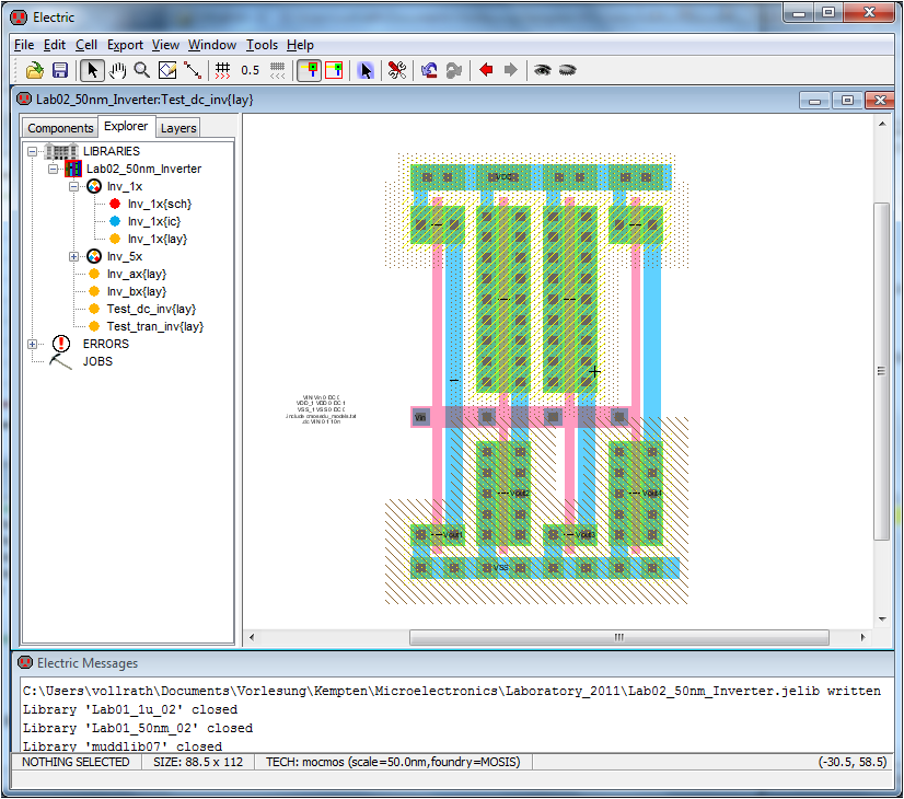
Check one of the cells for design rules DRC. PFETs should be 2 by 10 and NFETs 2 by 7.
There are 4 Inverters in the library: inv_1x1, Inv_a, Inv_b, inv_3x1.
- What is the difference between inv_1x1, Inv_3x1, Inv_ax and Inv_bx?
Design an inverter cell inv_9x1 with 9 unit transistors in parallel.
- Copy one of the cells and modify it. (Copy cells in group).
- The height and position of vdd and gnd of the new cell should be the same as the other cells.
- Do DRC frequently.
- For each external pin create the exports (vdd, gnd, vin, vout).
vdd and gnd exports are using M1. vin and vout exports should use a M1/M2 contact. - With the CTRL key you can cycle through the selection.
- With the Eye icon you can enable the display of the cell contents.
Select a cell. The outer bounds are higlighted and then click on the eye tool.
Sometimes you have to do it multiple times to see the underlying layout. - Choose a grid of 0.5 to be able to align the cells properly.
- Note down the area for Inv_9x1. What is the area per transistor? (in F2)
- Create a corresponding schematic for Inv_9x1. Insert the schematic into your report.
- To be able to use the schematic hierarchically an icon {ic} is needed. Create a corresponding cell{ic} for Inv_9x1 (View, Create icon view). Insert the exports.
Under tab 'Components' select 'Cell' and select your cell.
To look at the details of the cell use the Eye icon.
There are 2 simulations available: InvChain_dc; InvChainlong.
Simulate an Inverter
Select InvChain_dc {lay}.
Simulate it with SPICE.
Look at the voltages vin, vout1..vout5.
Make a printout (softcopy) of the result. What do you see? Why are the curves shifted?
Select InvChainlong{lay}
Simulate it with SPICE.
Look at the voltages vin, vout1..vout8.
Make a printout (softcopy) of the result. What do you see?
Measure the delay between input and output of the individual inverter for rising and falling output by comparing the 50% level.
Summarize the results. What do you see?
Calculate the delay times using SPICE measurement directives like:
.MEAS TRAN T2_V0750 WHEN V(vout7)=V(VDD)/2 FALL=1Measure (.MEAS) in the transient simulation (TRAN) the time value named T2_V0750, when (WHEN) the voltage vout7 (V(vout7)) equals 0.5V at the first falling transition (FALL=1).
Each measurement value needs a unique label.
Use the LTSPICE Help function to look for .MEAS.
A propagation delay can be calculated using for example:
.MEAS TRAN PROP7 PARAM T2_V0750-T2_V0650For each output voltage include a SPICE command to measure the transition times.
You can see the transition times in LTSPICE using View -> SPICE Error Log.
Copy the results to an editor or Excel and generate a table and/or graph.
Technology simulation
Redo the simulation and parameter extraction with the technology and parameters below.Change the scale for the technology and the transistor model include file. Do not change the layout.
Change the operation voltage and pulse voltage.
Make sure that the correct transistor model is used.
| Technology | Simulation file | VDD | L = 2 * scale | L = 2 * (1.1 * scale) | L = 2 * (1.2 * scale) | L = 2 * (1.3 * scale) | L = 2 * (1.4 * scale) | L = 2 * (0.9 * scale) |
| 1 µm | 1000nm_cmosedu_models.txt (3) | 5 V | ||||||
| 50 nm | 50nm_cmosedu_models.txt (54) | 1 V | ||||||
| 800 nm | 800nm_Holberg.txt (3) | 5 V | ||||||
| 500 nm | 500nm_Sedra.txt (1) | 3.3 V | ||||||
| 250 nm | 250nm_tsmc_level3.txt (3) | 3.3 V | ******38 BA | ******08 LK | *******28 MH | ******86 MN | ******11 BA | ******14 MV |
| 180 nm | 180nm_bulk.txt (49) Bad | 3.3 V | ******80 ZJ | ******22 LG | *******35 TT | ******76 AM | ******60 SS | ******16 SJ |
| 180 nm | 180nm_tsmc.txt (49) | 3.3 V | ******08 RM | ******80 GD | *******38 LR | ******89 DM | ******11 JA | ******97 HL |
| 130 nm | 130nm_bulk.txt (49) | 2.5 V | ******98 DG | ******20 DI | *******83 VN | ******92 AA | ******23 KS | ******08 SB |
| 90 nm | 90nm_bulk.txt | 1.8 V | ******13 GA | ******33 TG | *******96 JA | ******03 UM | ******36 SS | ******26 MT |
| 65 nm | 65nm_bulk.txt | 1 V | ******83 AI | ******46 TK | *******08 KV | ******02 RM | ******06 AF | |
| 22 nm | 22nm_ptm.txt | 0.9 V | ******26 SS | ******62 PV | *******11 SH | ******28 MM | ******22 PL | |
| 16 nm | 16nm_HP.pm.txt | 0.7 V | ******39 PS | ******15 AM | *******28 IA | ******08 DM | ******44 MM |
Report
The report should follow the same document format and have 1 page text and data and 1 page with your picture and background. The report should include:1) Delay data in graphical and/or tabular format.
2) Discussion of delay data.
3) Your experience during the practical training.
4) What obstacles did you experience how did you solve them?
5) You should also note down times you spent for each task.
Please send your electronic report (pdf) including your names, group number and lab number in the file name to joerg.vollrath@hs-kempten.de. The filename should be <date:yyyy_mm_dd>_Lab03_ <LastName>.pdf.
Please obey the names rule, do not zip or tar the files.
You can use PDFCreator for creating pdf files via the print menue in Windows.
Submission is due 07.06.2026 via email.