Elektronik 310 SpannungsreglerL‰ngsreglerProf. Dr. Jˆrg Vollrath09 Hallsensor |

|
Video der 16. Vorlesung Schaltungstechnik 18.5.2021
|
L‰nge: 1:02:43 |
0:2:16 5.1 Power overview 0:4:26 5.2 Power converters 0:6:2 5.3 Need for converters 0:8:18 Load Regulation 0:11:30 Line Regulation 0:13:55 Wirkungsgrad, Efficiency 0:14:39 5.4 DC Power Distribution PC 0:19:20 5.5 Types of Converters 0:24:20 DRAM power grid 0:29:30 Power on sequence 0:35:50 Linear regler, standard and LDO 0:37:0 5.7 Pros and Cons 0:41:4 Beispiel L‰ngsregler (Linearregler) 0:49:10 Diskussion Ergebnis 0:52:35 Welligkeit, ripple 0:55:0 5.9 Board space 0:57:44 5.11 PFET as pass device 1:1:40 5.13 Freilaufdiode 1:2:44 5.15 Stabilit‰t 1:5:20 LTSPICE Praktikumsschaltung 1:11:20 Last‰nderung am Ausgang 1:13:28 Load regulation LoR = 30mV/300mA = 0.1 Ohm 1:15:55 Spannungsverlauf bei Last‰nderung 1:18:40 Stabilit‰t |
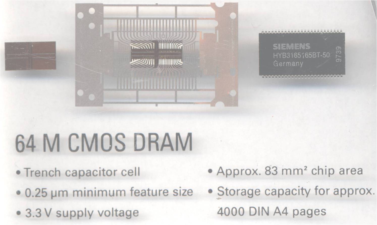
Power grid: DRAM example
|

|
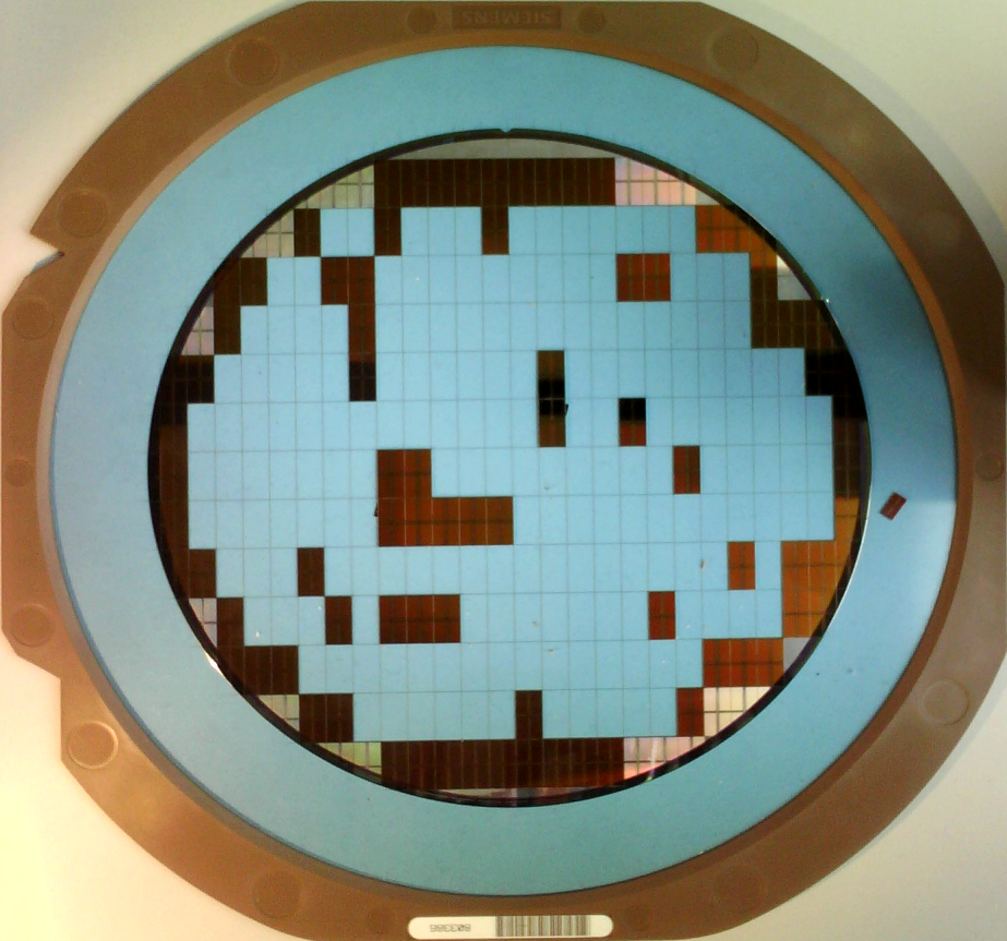
Power grid: DRAM example

|
|
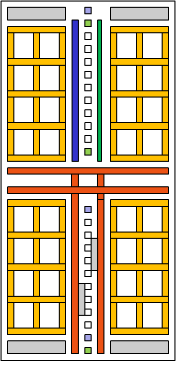
There are separate power supply pins for the data input and outputs (IO).
The number of power pins is proportional to the number of IOs.
There are separate grids for digital and analog circuits.
Horizontal and vertical lines are connected to a grid and provide power.
The block diagram shows different voltages in different colors in different areas.
Voltage pumps and regulators are shown in grey.
A bandgap reference circuit provides temperature and voltage independent voltages.
Power on sequence: DRAM

|
A low array voltage is used to save power.
A negative back bias is needed reducing memory cell leakage current.
A high voltage Vpp gives the select transistor overdrive to store the full Vblh level in the memory cell.
Vint is optimized for speed and to be able to drive the IOs.
A high current peak, when power is turned on, has to be avoided.
All capacitances will be charged up at power up.