Interface Electronics03 Ideal ADC, DNL and INLProf. Dr. Jörg VollrathPrevious: 02 LTSPICE |
Video 3. lecture
|
Länge: 01:06:27 |
0:0:0 Start 0:1:22 ADC Converter metric 0:3:23 ADC transfer characteristic 0:4:40 First transition half LSB 0:6:35 2^n codes, 2^n-1 transitions, 2^n-2 steps 0:8:17 Transition table 0:9:15 Offset and gain error of ADC 0:11:39 Differential non linearity DNL 0:14:37 3-bit, 8 codes, transitions 7, steps 6 0:17:16 DNL calculation 0:17:48 Sum DNL is zero 0:18:50 Integral non linearity INL 0:19:44 measurement of INL and DNL 0:21:32 Histogram test 0:26:30 INL sum of DNL 0:28:25 ADC Error simulator 0:29:11 Simulator ideal ADC ramp result 0:31:55 Introducing an distortion error 0:32:34 Transfer curve INl, DNL 0:35:29 Exam WS2010 Problem 1 0:36:50 LSB =(VMAX-VMIN)/(2^n-2) = (1.21-0.09)/14 V = 0.08 V 0:39:3 Math Notepad 0:39:45 Offset error 0.09-0.08/2 = 0.05 V 0:42:50 INL and DNL 0:44:13 INL(0100) = 0.525 0:46:0 DNL(0100) = 0.2 0:48:22 WS2011 Problem 1 Histogram 0:49:10 Don't use first and last occurences 0:50:0 navg = 15 0:50:59 DNL(1) = -0.2 0:52:0 DNL(2) = 0 0:53:0 INL(1) = -0.2 0:55:0 Resolution of histogram test 1/15 0:56:45 Simulator 0:57:27 INL, DNL simulation with noise 1:0:0 8-bit simulation 1:2:50 small distortion 1:4:40 Sine input for histogram 1:7:40 Number of samples for sine histogram 1:10:43 Characterization system 1:14:15 WS2011 Problem 1 DAC 1:15:30 Excel data 1:16:10 First and last ideal voltage 1:16:30 LSB calculation 1:17:28 Ideal output voltages 1:18:24 LSB accuracy 1:19:37 DNL calculation 1:20:40 INL calculation 1:22:12 Plotting transfer curve 1:24:2 Plotting INL, DNL |
Review and Overview
Review
- Properties of digital signals
- Applications of data converters
- DAC metric: N, D, Vmax
- LTSPICE basic operation:
- R,L,C,V,M,Q,X components
- simulation: .op .dc .tran
- LTSPICE data converter simulation
Overview
- ADC metric: N, D, Vmax
- Static errors: Offset, gain, INL, DNL
- Histogram test with ramp and sine signal
Baker:
Holberg:
AD Converter Metric
|
N: Number of Bits D0..DN-1: Binary weighted data lines Vin: Positiv input voltage Vmax: Maximum input voltage VFS: Full scale voltage Vref: Reference voltage Δ = LSB: minimum resolvable input For small N there is a significant difference LSB or Δ between Vmax, VFS and Vref. In general \( V_{max} = V_{FS} = V_{ref} - LSB \) (Baker). For large N, LSB gets small and Vmax = VFS ≈ Vref. |
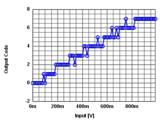
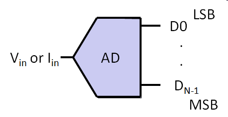 Ideal analog-to-digital converter An analog voltage or current is transfered into a digital output. Input range is positiv. Uniform, binary digital encoding |
AD Transfer Characteristic
|
Transition depends on measurement accuracy and step size. |
Vref = 1V N = 2 LSB = 0.25V Upper voltage limit (transition voltage) for a digital output code:
|
Analog-Digital-Converter (ADC)
N: Number of bits
Vref: Reference voltage
Example: N = 12, Vref = 4 V
\( LSB_{rel} = \frac{1}{2^{12}} = \frac{1}{4096} = 0.00024414 = 244 ppm \)
\( LSB_{abs} = \frac{4 V}{2^{12}} = \frac{4 V}{4096} = 976.56 uV \)
We are using LSBabs.
Attention rounding of LSB:
4095 * 976.56 uV = 3.999 V
4095 * 976 uV = 3.996 V
3 mV Difference in calculation versus LSBabs 0.976 mV
Static Errors
|
Offset Error, Gain Error Offset and gain error will be fixed during manufacturing. A trimmable amplifier is used. In this lecture first the LSB or Δ is calculated from the first and last points of the transfer curve. Then the offset is calculated for the first code or first transition voltage. Then static errors differential non linearity (DNL) and integral non linearity (INL) are calculated. |
\( LSB = \frac{ V_T (10/11)_{real} - V_T (00/01)_{real}}{2^{N}-2} = \frac{ 2 V }{ 2} = 1 V \)
Offset error: Voffset = VT(00/01) - 0.5 LSB = 0.3 V - 0.5 V = - 0.2 V
Gain error: \( V_{gain} = \frac{(V_T (10/11)_{real} - V_T (00/01)_{real})} { (V_T (10/11)_{ideal} - V_T (00/01)_{ideal}) } = \frac{2.25 V - 0.45 V}{2.5 V - 0.5 V} = 0.9 \)
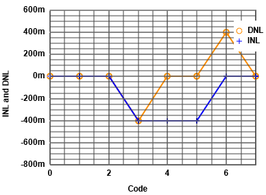
DAC Differential non linearity (DNL)
Differential non linearity characterizes the step size (difference) between 2 successive codes.
|
Step size:
\( LSB = \frac{V(111) - V(000)}{2^{3}-1} = 1 V \) The step size between 2 successive codes is normalized with LSB and calculated as DNL: \( DNL(n) = \frac{ V(n) - V(n-1) - LSB}{LSB} \) Since the LSB is calculated using the first and last code: \( \sum DNL_i = 0 \) |
The graph and the table represent the same data and contain the same information.
The ideal curve is calculated starting with Vmin(code=000), addding LSB for each step and ending at Vmax(code=111).
The ideal curve is calculated starting with Vmin(code=000), addding LSB for each step and ending at Vmax(code=111).
DAC Integral non linearity (INL)
Integral non linearity characterizes the difference real and ideal transfer characteristics.|
Step size: \( LSB = \frac{V(111) - V(000)}{2^{3}-1} = 1 V \) The difference between real and ideal curve is normalized with LSB and calculated as INL: \( INL(n) = \frac{ V_{real}(n) - V_{ideal}(n)}{LSB} \) Since the INL is calculated using the first and last code: INL(000) = 0; INL(111) = 0; |
The error of the output voltage should be less than ±1/2 LSB.
-1/2 LSB > INL > 1/2 LSB
How to measure INL and DNL?
DAC:Apply digital code and use a good voltmeter to measure corresponding analog output.
Noise can be filtered with averaging.
ADC:
Transition voltages have to be measured.
Noisy transitions.
Provide slow ramp and measure transition voltage.
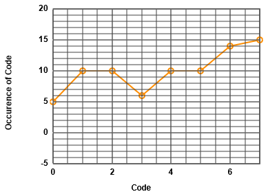
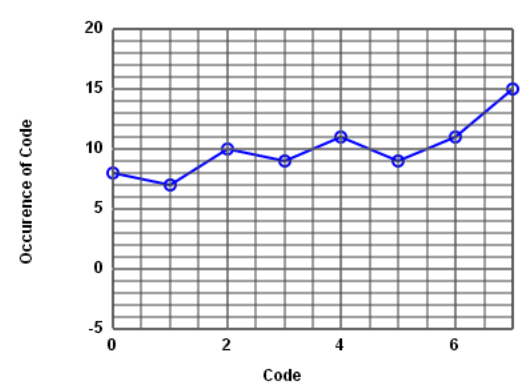
Histogramm test
|
Apply input voltage ramp over time. Measure number of occurence of each output code. With a constant ramp slope (RS [V/s]) an ideal ADC with a sampling frequency fs and a step size of LSB gives: \( n(code) = \frac{LSB}{RS} \cdot f_s = n_{avg} \) Ideally n is constant for the input voltage range except for the first and last code. DNL can be calculated as: \( DNL(code) = \frac{n(code) - n_{avg}}{n_{avg}} \) INL is: \( INL(code) = \sum_{i=0}^{code} DNL(i) \) The accuracy for INL and DNL of this test is: \( \frac{1}{n_{avg}} \) |
The test time is:
\( \sum_{code = 0}^{2^{N}-1} n(code) \cdot \frac{1}{f_s} = 2^{n} \cdot n_{avg} \cdot \frac{1}{f_s} \)
\( \sum_{code = 0}^{2^{N}-1} n(code) \cdot \frac{1}{f_s} = 2^{n} \cdot n_{avg} \cdot \frac{1}{f_s} \)
Histogramm test example with error
Number of Bits: 3Zoom transfer: Start voltage: 0, Number of samples 80
Distortion: amplitude 0.05, start 0.3, length 0.4
ADC Characteristic
Histogramm test with sine input signal
|
Higher resolution DAC Filter Occurence bathtub shape Range matching |
This example shows a 4 Bit test using 400 measurement points.
It is difficult to build an analog linear ramp generator.
A higher resolution DAC can be used.
A sine input signal can be used.
A high quality filter eliminates harmonics.
Occurence will not be flat, but can be calculated in advance to normalize occurence to calculate INL and DNL.
Occurence has a bathtub shape.
At top and bottom highest occcurence can be seen, since the sine signal is flat.
In the center low occurence can be seen due to the high slope of the sine signal.
It is difficult to match the sine signal exactly to the input range of the ADC.
Histogramm sine signal
|
How many samples M do you need of a sine input signal for a N Bit data converter? There will be more samples available at the top and bottom and less in the center. Signal: \( V(t) = 2^{N-1} \cdot LSB \cdot sin \left( \omega t \right) \) Amplitude is: \( 2^{N-1} \cdot LSB \) \( V'(t) = 2^{N-1} \cdot LSB \cdot \omega \cdot cos \left( \omega t \right) \) \( M_{min} \approx 3 \cdot 2^N \) |
Maximum change in signal after dt should be smaller than LSB:
\( 2^{N-1} \cdot LSB \cdot \omega \cdot dt \lt LSB \)
with \( \omega = \frac{ 2 \pi}{M dt} \)
\( M \gt 2 \cdot \pi \cdot 2^{N-1} \approx 3 \cdot 2^N \)
Having 16 times 2N samples gives an accuracy for INL and DNL of \( \frac{3}{16} \approx 0.2 \).
Having 8 times 2N samples gives an accuracy for INL and DNL of \( \frac{3}{8} \approx 0.375 \).
Histogramm sine signal accuracy
Error in sine signal estimateMake sure integer number of periods are used. A slight error in estimation of number of periods, amplitude and offset of sine signal can lead to codes in the limited range of ADC having big INL and DNL errors. Fit a curve with minimum error. Bits: 5 Range: 0..31 1) Average shift: - 0.4LSB 2) Amplitude increased: + 0.4LSB |
Y = round((2^(n-1) - 0.5) + (2^(n-1) - 0.5) * sin(x*11/gr*2PI)) ;
Y = round((2^(n-1) - 0.9) + ((2^(n-1) - 0.5) * sin(x*11/gr*2PI))) ;
Y = round((2^(n-1) - 0.5) + ((2^(n-1) - 0.1) * sin(x*11/gr*2PI))) ;
Y = round((2^(n-1) - 0.9) + ((2^(n-1) - 0.5) * sin(x*11/gr*2PI))) ;
Y = round((2^(n-1) - 0.5) + ((2^(n-1) - 0.1) * sin(x*11/gr*2PI))) ;
Histogramm sine signal practical test setup
A real Histogram implementation needs RAM:- Sine signal buffer: \( 2^{N} \cdot 4 \cdot N \)
- Error correction lookup DAC: \( 2^{N} \cdot N \)
- Error correction lookup ADC: \( 2^{N} \cdot N \)
- Output buffer: \( 2^{N} \cdot 16 \cdot N \)
A NEXYS3 Spartan 6 xc6slx16 FPGA board has 32 Blocks of 18Kbit block RAM.
This allows a 10 Bit converter to be implemented in FPGA: \( 2^{10} \cdot 22 \cdot 10 \approx 23 \) blocks.
NEXYS3 external 16MByte Cellular RAM: 16 Bit asynchronous 70ns (14 MHz), synchronous 80 MHz.
Read sine from lookup in 83 ns, read SAR output and get lookup corrected output, store corrected output.
250ns cycle time: 83ns each, 4 MHz
16 Bit: 65k * 22 * 16 = 1365kBit * 16 = 2.8 MByte
18 Bit: 256k * 22 * 18 = 12 MByte
Up to 18 Bit at 4 MHz are possible with external RAM.
When is a CORDIC sine calculation better than a lookup table?
Characterization System
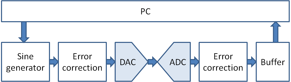

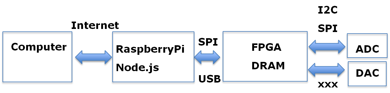
IEEE Data converter Measurement
IEEE standards 1241 and 1057 [2] [3]
describe the most effective ADC testing procedures to apply for evaluating figures of merit of such devices. Methodology usually employed are based on the analysis of data generated at the ADC output when a spectrally pure single- or dual-tone is applied to the input of the device under test (DUT).
European draft standard Dynad 131 not found via internet
Practical Histogramm Testing
- Histogramm test assumes monotonicity.
- Testing many devices gives statistical and systematic error.
- Always look at DNL and INL.
- Even with a low DNL INL can be quiet high by accumulating DNL error.
Tasks and Next:
WS2011 Problem 1 DAC INL, DNL
WS2010 Problem 1 ADC INL, DNL
WS2012 Problem 1 ADC Histogram
Dynamic testing
04 Spectral test
References:
[1] M. V. Bossche, J. Schoukens, and J. Renneboog, “Dynamic Testing and Diagnostics of A/D Converters,” IEEE Transactions on Circuits and Systems, vol. CAS-33, no. 8, Aug. 1986.[2] IEEE Standard 1057
[3] IEEE Standard 1241
IEEE Std 1241