Interface Electronics02 SPICEProf. Dr. Jörg Vollrath01 Introduction and basic properties |

|
Video 2. lecture
|
Länge: 01:06:27 |
0:0:0 Review Introduction 0:0:44 Video recording 0:1:34 LTSPICE start 0:2:49 LTSPICE configuration white background and thick lines 0:5:13 Thick lines 0:7:29 Start schematic with resistor 0:8:44 Finished low pass placing parts 0:12:12 Values for components 0:12:44 Labels node names 0:13:19 Simulate .op 0:14:59 Turning a resistor changes polarity of current 0:16:12 Simulate .dc voltage ramp 0:17:1 Add trace to graph 0:18:44 Sine voltage at source 0:19:44 Transient simulation .tran 0:20:30 Graph discussion 0:21:6 Higher frequency 0:22:36 AC simulation, voltage source and command 0:24:14 Graph discussion 0:25:6 Corner frequency 0:26:56 Context sensitive menues 0:27:36 Measure command .MEAS 0:28:54 Verification of result 0:30:13 Data converter schematic 4 Bit DAC 0:31:36 Copying SPICE code to local drive 0:32:36 Copying subcircuits .asc .asy 0:33:56 ADC circuit download 0:34:37 ADC DAC test circuit 0:35:33 Explanation test circuit 0:36:33 Hierarchie 0:37:18 Sample and hold 0:38:43 .Save command 0:40:13 16 steps 0:41:53 Voltage probe 0:42:23 High frequency sampling 0:44:25 12 Bit test circuit 0:45:58 Tools for data processing and analysis 0:47:28 Webreport 0:48:28 Directories and files 0:51:1 Presentation and handout mode 0:51:33 Editor 0:53:28 HTML tags 0:55:11 LTSPICE schematics from files 0:57:44 Equations with MathJax 0:58:19 Animations 0:59:53 Insert images 1:1:33 Copy, paste, modify |
SPICE
|
|
LTSPICE: First Steps
|

|
LTSPICE: Configuration
|


|
Example Voltage divider operation point: .op
Schematic

|
Netlist
|
Voltage source variation: .dc Vin 0 1 1m
Schematic 
|
Netlist
|

SPICE: Sinusodial source
|

|
Transient simulation: .tran 1n 3u
|
Schaltplan |
|
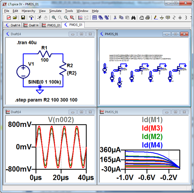
MOSFET transistors in LTSPICE
Netlist:M1 NDrain NGate NSource PBulk NMOSModel
M2 PSource PGate PDrain PBulk PMOSModel
.model NX NMOS(LEVEL=1 KP=300u
+ VT0=0.8 LAMBDA=0.000 CGDO=400n)
.lib C:\Program Files (x86)\LTC\LTspiceIV\lib\cmp\standard.mos
.include cmosedu_models.txt
Example:
M1 VD VG VS VB N_50nm
The transistor model N_50nm can be specified in a model statement (.model), can be supplied in a library file (.lib) or in an external file (.include)
Symbol:

Transistor measurement
LTSPICE: Hierarchy
|

|
Hilfe LTSPICE für Temperaturvariation: Suchbegriff R, TEMP

Simulation with varying components
|

|

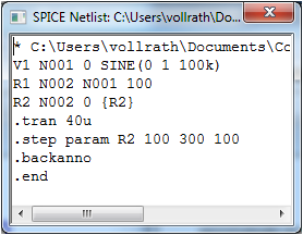
Test for 4 Bit ADC and DAC
|
A 4 Bit ADC and DAC test can be simulated in LTSPICE. The output file size can be limited by using the .save dialog option. The output shows the step size of the digitalisation. 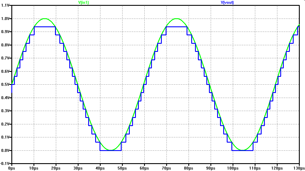
|
Test for 12 Bit ADC and DAC
|
A 12 Bit ADC and DAC test can still be simulated in LTSPICE.
The output file size can be limited by using the .save dialog option. FFT 65k points gives: signal: -9dB, noise level: -116dB Calculation: 6.07 * B dB + 1.76 dB + 10 log(N/2) dB = 6.07 * 12 dB + 1.76 dB + 10 log(65k/2) dB = 72 dB + 1.76 dB + 45 dB = 119 dB 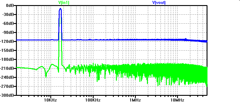
|
Analyzing this data with
Read LTSPICE raw file for data converter analysis.
with Start = 0, Stop = 655.36E-6, Step 10E-6
and procesing integer values with
FFT and INL, DNL data converter analysis
gives you less SQNR than expected due to sample and hold circuits distroting the residue.
A comparison of the signals res0 and vout0, res1 and vout1 shows the performance of the circuit. The signals should be identical.
It is unclear why the FFT in LTSPICE is not showing this.
A comparison of the signals res0 and vout0, res1 and vout1 shows the performance of the circuit. The signals should be identical.
It is unclear why the FFT in LTSPICE is not showing this.
Improved Test for 12 Bit ADC and DAC
|
A 12 Bit ADC and DAC test can still be simulated in LTSPICE.
The output file size can be limited by using the .save dialog option. Sample and hold circuits are only used at the input and output. Javascript FFT 16k points gives: signal: 84.3dB, noise level: 8.56dB Calculation: 6.07 * B dB + 1.76 dB + 10 log(N/2) dB = 6.07 * 12 dB + 1.76 dB + 10 log(16k/2) dB = 72 dB + 1.76 dB + 40 dB = 119 dB 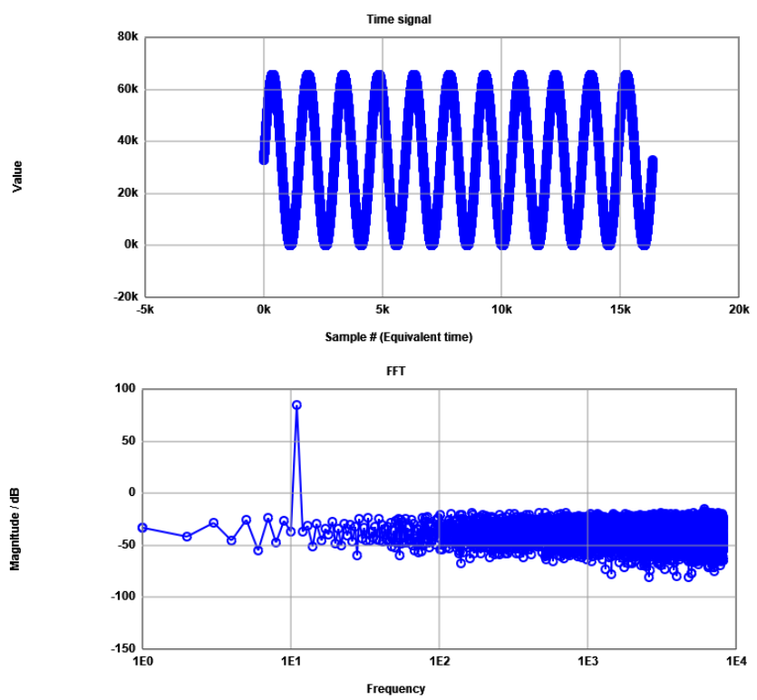
|
Start time 0, Stop time 655.36E-6, Time step 40E-9 gives 16384 data points.
Mapping this with a scale of 65535 to integer prepares analysis with Javascript FFT.
Mapping this with a scale of 65535 to integer prepares analysis with Javascript FFT.