Interface Electronics08 ADC Sampling and ErrorProf. Dr. Jörg Vollrath07 DAC practical examples |
Video Lecture: ADC Architectures
|
Länge: 01:06:27 |
0:0:0 Sine histogram by hand 0:0:50 Values in histogram 0:1:22 Pivot table 0:2:34 Sine occurences 0:3:0 Reference 11 periods 0:6:0 Pivot of reference 0:8:45 DNL equation 0:9:14 INL equation 0:10:12 Reference amplitude error 0:12:0 Verification comparing 2 tools and solutions 0:12:56 Laboratory 4 Arduino with ADC, DAC measurement 0:20:14 DAC summary settling time 0:22:34 Timing error 0:23:19 RC low pass 0:24:5 ADC architectures Flash, Pipeline, SAR, Sigma Delta, Dual slope 0:25:37 Resolution and speed 0:28:59 Trade off speed and resolution 0:30:12 ADC Architectures 0:30:59 ADC Signal Chain 0:34:4 ADC Architectures 0:35:31 Ideal Sampling 0:37:37 Real Sampling Switch 0:39:57 RC Time Constant 0:41:17 Clock coupling 0:42:22 Low pass R, C requirement 0:43:41 Upper limit R for speed 0:45:1 Low pass requirement table 0:48:22 R < 0.72/B/fs/C equation 0:50:32 Clock bootstrapping 0:54:25 Clock feed through 0:57:45 Clock feed through compensation 0:59:22 Fully differential sampling 1:0:35 Track and hold sample and hold 1:1:10 Clock jitter 1:4:37 Jitter requirements 1:7:22 Jitter simulation 1:10:7 Spectrum and Jitter analysis 1:10:49 ENOB and Jitter 1:12:43 Summary |
Review and Overview
- ADC architectures, resolution and conversion rate
- AD conversion
- Sampling
- RC circuit
- kT/C Noise
- Acquisition bandwidth
- Switch on resistance
- Bootstrapping
- Fully differential realization
- Clock jitter
Statistical analysis
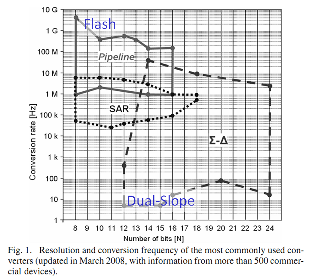
ADC architectures, resolution and conversion rate
A graph with x axis frequency and y axis resolution shows applications.
Pipeline ADC: 8..16 Bits, 1MHz..4GHz
SAR ADC: 8..18 Bits, 20kHz..8MHz
Sigma Delta ADC: 12..24 Bits, 4Hz..40MHz
Source: QUINTÁNS et al.: METHODOLOGY TO TEACH ADVANCED A/D CONVERTERS, IEEE TRANS. ON EDUCATION, VOL. 53, NO. 3, AUGUST 2010
Investigation of distributer Digikey (01/2017):
Flash ADC (Results: 366): 10 Bit 50 MSps, Range 3..16Bit, 50kHz..26GHz
8 Bit 50kHz AD782 ADI, 3Bit 26GHz HMCAD5831LP9BE ADI, 8 Bit 1GHz MAX104CHC Maxim 16 Bit 166kHz AD7884AQ ADI
Pipeline ADC (Results: 3237): 12 Bit 125MSps, Range 6..16 Bit, 94k..2.6GHz
12 Bit 94kHz MAX1253BEUE+, 12 Bit 2.6GHz ADI, 6 Bit 90MHz MAX1011, 16 Bit 1GHz ADS54 TI
SAR ADC (Results: 8973): 12 Bit 1MSpS, Range 8.. 32Bit 1kSps..500 MSps
32 Bit 1MSps LTC2508 $16, 24 Bit 2MSps LTC2380 $54, 20 Bit 1.6 MSps MX11905 $30 8 Bit 500MSps ISLA118P5 Intersil $50, 8 Bit 3MSps MAX 11116 $2
Sigma Delta ADC(Results: 1928): 24 Bit 256kSps Range: 8..32 Bit , 3Sps..3.2GSps
16 Bit 3.2GSps(100MHz) AD6676 ADI $200, 16 Bit 160MSps(2.5MHz) AD9262 ADI $48, 12 Bit 3.3kSps ADS1015 TI $2, 32Bit 1MSps LTC2508 $17
Dual Slope (Results: 28): 15 Bit 30Sps
ADC architectures, resolution and conversion rate
|
 Source: QUINTÁNS et al.: METHODOLOGY TO TEACH ADVANCED A/D CONVERTERS, IEEE TRANS. ON EDUCATION, VOL. 53, NO. 3, AUGUST 2010 |
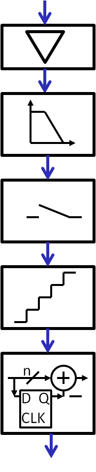
AD conversion signal chain
Analog signal|
Preamplifier (range adjustment, impedance matching) Anti-alising filter Sampling Quantization Digital coding (error correction, filter) |
 |
Ideal sampling
|
At at time t0 the external voltage is stored internally and fixed until t0+T. The fixed voltage is necessary for a successful conversion. The fixed voltage is necessary to really have the voltage at time t0. The fixed voltage can be easily converted with an ADC. A capacitor is used to store charge to sample the voltage. |
An ideal sample and hold can be used in LTSPICE to analyze switched waveforms. |
Real sampling
|
Transistor is used as a switch. A transistor is on for half the sampling period. During this time the signal is tracked. Then the transistor is turned off and the charge and voltage fixed on the capacitor. The transistor has a finite resistance, limiting the bandwidth of the RC circuit. The resistance has thermal noise which can limit the resolution (number of bits) of the ADC. The control clock of the gate of the transistor is capacitively coupling to the stored voltage. The transistor source has a leakage current discharging the capacitance. The input voltage source has to be able to drive enough current to charge the capacitance. |
Sampling network low pass thermal noise
A resistor has a noise voltage:\( \frac{V_{rms}^2}{\Delta f} = 4 k_B \cdot T \cdot R \)
A low pass RC network limits the noise to:
\( \overline{v_n^2} = \frac{k_B T}{C} \)
This noise has to be lower than the quantization noise:
\( \overline{v_q^2} = \frac{\Delta^2}{12} = \frac{V_{FS}^2}{2^{2B} \cdot 12}\)
Sampling network thermal noise capacitance requirement
\( C \gt 12 \cdot k_B \cdot T \frac{2^{2 B}}{V_{FS}^{2}} \)kB: Boltzmann constant (1.38 · 10 -23 m2kg s-2K-1)
T: absolute temperature in Kelvin
B: number of Bits
VFS: Full scale voltage
| B | Cmin(V |
Cmin(V |
| 8 | 0.3 fF | 0.003 pF |
| 12 | 80 fF | 0.8 pF |
| 16 | 20.6 pF | 206 pF |
| 20 | 5.28 nF | 52.8 nF |
| 24 | 1.32 uF | 13.2 uF |
Adding 4 bits required an increase in capacitance by a factor of 256.
Decreasing the voltage by a factor of 3.3 increases the capacitance with a factor of 10.
Sampling network low pass requirement
|
The sampling network has a transfer function of: \( \underline{T}(j\omega) = \frac{\underline{U}_a}{\underline{U}_e} = \frac{\frac{1}{j\omega C}}{R + \frac{1}{j\omega C} } \) \( \underline{T}(j\omega) = \frac{1}{j \omega C R + 1 } \) The difference in magnitude should be less than 1/2 LSB. Lets look at a normalized transfer function \( \Omega = \omega C R \) \( \underline{T}(j\Omega) = \frac{1}{j \Omega + 1 } \) |
To prevent gain error from the signal transfer function \( \frac{1}{| j \Omega + 1 |} \gt (1 - 0.5 \frac{LSB}{V_{ref}} ) \) \( \frac{1}{| j \Omega + 1 |} \gt (1 - \frac{1}{2^{B+1}} ) \) \( \Omega^{2} \lt \frac{1}{(1 - \frac{1}{2^{B+1}} )^2} - 1 \) \( \Omega \lt \frac{1}{2^\frac{B}{2}} \) \( 2 \pi \frac{f_g}{2} R C \lt \frac{1}{2^\frac{B}{2}} \) \( R \lt \frac{1}{\pi \cdot f_g \cdot C \cdot 2^\frac{B}{2}} \) |
To prevent gain error from the signal transfer function
\( \frac{1}{| j \Omega + 1 |} \gt (1 - 0.5 \frac{LSB}{V_{ref}} ) \)
\( \frac{1}{| j \Omega + 1 |} \gt (1 - \frac{1}{2^{B+1}} ) \)
\( \frac{1}{\sqrt{ \Omega^{2} + 1 }} \gt (1 - \frac{1}{2^{B+1}} ) \)
\( \frac{1}{(1 - \frac{1}{2^{B+1}} )^2} \gt \Omega^{2} + 1 \)
\( \Omega^{2} \lt \frac{1}{(1 - \frac{1}{2^{B+1}} )^2} - 1 \)
\( \Omega^{2} \lt \frac{1 - 1 + \frac{1}{2^B}- \frac{1}{2^{2B+2}}}{(1 - \frac{1}{2^{B+1}} )^2} \)
\( \Omega^{2} \lt \frac{\frac{1}{2^B} \left( 1 - \frac{1}{2^{B+2}} \right) }{(1 - \frac{1}{2^{B+1}} )^2} \approx \frac{1}{2^B} \)
\( \Omega \lt \frac{1}{2^\frac{B}{2}} \)
\( 2 \pi \frac{f_g}{2} R C \lt \frac{1}{2^\frac{B}{2}} \)
\( R \lt \frac{1}{\pi \cdot f_g \cdot C \cdot 2^\frac{B}{2}} \)
Sampling network low pass requirement table
| Bits, frequency [fg] | Ua [V] | 1 - 20*log(Ua) |
| ∞ ,DC | 1 | 0 dB |
| 24, 0.00024 | 0.99999994 | -0.0000006 dB |
| 20, 0.0097 | 0.99999905 | -0.000008 dB |
| 16, 0.0039 | 0.999985 | -0.00013 |
| 12, 0.0156 | 0.9976 | -0.0021 |
| 8, 0.0625 | 0.996 | -0.034 |
Sampling network voltage difference requirement
The capacitor has to be charged to the 1/2 LSB range of the input voltage:\( | V_e - V_a | < 0.5 LSB \)
The voltage on the capacitor is:
\( V_a = V_e \cdot \left( 1 - exp^{-\frac{t}{\tau}} \right) \) with \( \tau = RC \)
This gives:
\( V_e - V_e \cdot \left( 1 - exp^{-\frac{t}{\tau}} \right) < 0.5 LSB \) \( V_e \cdot e^{-\frac{t}{\tau}} < 0.5 LSB \)
Maximum difference could be full scale \( V_e = 2^{B} \cdot LSB \) with B number of bits:
| \( 2^{B} \cdot LSB \cdot exp^{-\frac{t}{\tau}} < 0.5 LSB \) | \( exp^{-\frac{t}{\tau}} < 2^{-N-1} \) |
| \( -\frac{t}{\tau} < ln \left( 2^{-B-1} \right) \) | \( -\frac{t}{\tau} < \left( -B-1 \right) ln \left( 2 \right) \) |
| \( t > R C \left( B+1 \right) ln \left( 2 \right) \) |
\( R < \frac{1}{2 \cdot f \cdot C \left( B+1 \right) ln \left( 2 \right) } = \frac{0.72}{ f_{sample} \cdot C \left( B+1 \right) } \)
Sampling network voltage difference resistance requirement
\( R \lt \frac{0.72}{B \cdot f_s \cdot C} \)fs: Sampling frequency (half period active and switch closed)
B : number of bits
C: sampling capacitance
Since these values are very low and can not be realized, higher values are used and a digital filter or error correction is required to adjust the frequency response.
This process with the measured RDSon in the range of kΩ can realisticly achieve:
1GHz, 10 Bit;
100 MHz, 12 Bit;
10 MHz, 14 Bit;
Clock bootstrapping
Achieve a constant resistance of the switch by using a constant overdrive.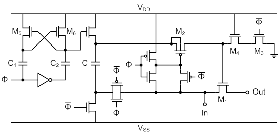
Ref: A. M. Abo and P. R. Gray, “A 1.5-V, 10-bit, 14.3-MS/s CMOS pipeline ADC,” IEEE Journal of Solid-State Circuits, vol. 34, issue 5, pp. 599-606, 1999.
Clock feed through
|
The clock signal is coupling via the switch transistor capacitance to the signal. Voltage coupling depends on load capacitance. A charge is specified. Example: TI switch: ts3a44159 |
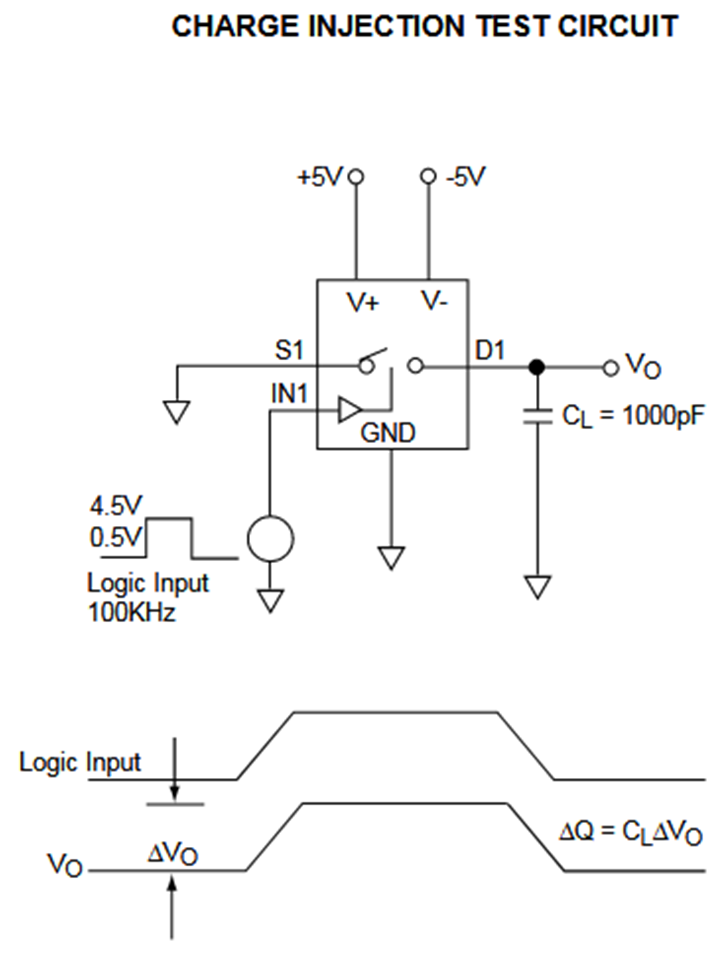 Source: data sheet ALD4201/ALD4202M Advanced Linear devices |
Clock feed through compensation
|
Compensation with dummy transistors:
|
The following imperfections occur:
Capacitive coupling from clock to the input and output.
Charge during the on state in the channel has to be compensated.
CLK and CLKb have to symmetric. Use a real clock signal from an inverter to estimate asymmetry.
Capacitive coupling from clock to the input and output.
Charge during the on state in the channel has to be compensated.
CLK and CLKb have to symmetric. Use a real clock signal from an inverter to estimate asymmetry.
Fully differential sample and hold
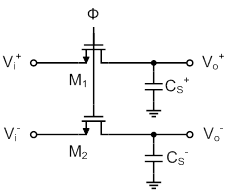
FullyDifferentialTH
Clock jitter and signal sampling
|
Random variations in the period of the clock is called clock jitter.
This can happen due to power noise or signal noise.
Long lines and buffer stages can increase clock jitter. What errors are induced by clock jitter? INL, DNL, signal to noise ratio. The yellow curve shows the ideal waveform. Clock jitter causes to sample data earlier or later (green curve). This causes error due to the change in signal level (blue curve). This causes error (red curve) reflected in INL, DNL and signal to noise ratio. |
|
Clock jitter requirements
|
What are requirements for clock jitter? Clock jitter has to be smaller than 1 LSB. Signal: \( V(t) = 2^{N-1} \cdot LSB \cdot sin \left( \omega t \right) \) Amplitude is: \( 2^{N-1} \cdot LSB \) The slope is: \( V'(t) = 2^{N-1} \cdot LSB \cdot \omega \cdot cos \left( \omega t \right) \) Maximum change in signal after dt should be smaller than LSB: \( 2^{N-1} \cdot LSB \cdot \omega \cdot dt \lt LSB \) \( dt \lt \frac{1}{2 \cdot \pi \cdot f_{signal} \cdot 2^{N-1} } = \frac{1}{ \pi \cdot f_{sampling} \cdot 2^{N} } \) Higher signal frequency or greater amplitude will increase the signal change after dt and increases jitter errror. | Clock accuracy timing requirement in s |
Statistical jitter analysis
Calculation of the mean squared jitter error (variance)sinusoidal signal
x(t) = A sin(2 π fx t)
then
x’(t) = 2 π fx A cos(2 π fx t)
E{[x’(t)]2} = 4 π 2 fx2 A 2
Jitter variance E{(tJ-t0) 2 } = σ 2
If x’(t) and the jitter are independent
– E{[x’(t)(tJ-t0)] 2} = E{[x’(t)] 2} E{(tJ-t0) 2}
Hence, the jitter error power is
E{e2} = 4 π2 fx2 A2 σ2
If the jitter is uncorrelated from sample to sample, this “jitter noise” is white
\( DR_{jitter} = \frac{\frac{A^2}{2}}{2 \pi^2 f_x^2 A^2 \sigma^2} \)
\( DR_{jitter} = \frac{1}{2 \pi^2 f_x^2 \sigma^2} \)
\( ADR_{jitter} = - 20 log_{10} \left( 2 \pi f_x \sigma \right) \)
DR: Distortion ratio
Ratio of power of Sine signal and power of jitter noise.
A: Amplitude
fx: frequency
σ2:jitter variance
Spectrum and jitter analysis
|
Clock jitter has a spectrum and degrades the signal to noise ratio. Clock jitter can be simulated: AD Characteristic The jitter error is specified with standard devitation regarding sampling clock period. To have errors smaller than one period the error should eb smaller than 0.1 The signal has an offset of 0.5 and an amplitude of 0.5. This gives -9 dB for the signal. |
Simulated total noise level with jitter: ADC Simulation
Signal: -9.03 dB Quantization noise level: -58 dB Change in std deviation of factor of 2 gives 6 dB, one bit. |
ENOB and jitter
|
Calculate signal to noise at different frequencies. If you have frequency dependent signal to noise ratio calculate jitter variance. Problem for subsampling. ADC Simulation 17,53,173,601 and 1731 periods. Noise error:0.1, 0.05, 0.005 Math.sin((i + jitter * randomNormal(0.5) ) / Npair * 2 * Math.PI * nPeriod) |
Summary
- Pick a capacitor according to the resolution of the ADC
- Select a low resistance for the switch
- Clock coupling should be measured
- Both can be compensated by digital filtering and error correction
- Jitter can limit the signal to distortion ratio and should be eliminated with careful clock design.
- Jitter can be identified measuring noise level with varying signal amplitude and frequency.
- Use appropriate capacitances for all signal nodes and power supply.
- Differential signaling can minimize external signal interference.
References
Resitor thermal noise: https://en.wikipedia.org/wiki/Johnson%E2%80%93Nyquist_noise
Next:
09 ADC Architecture