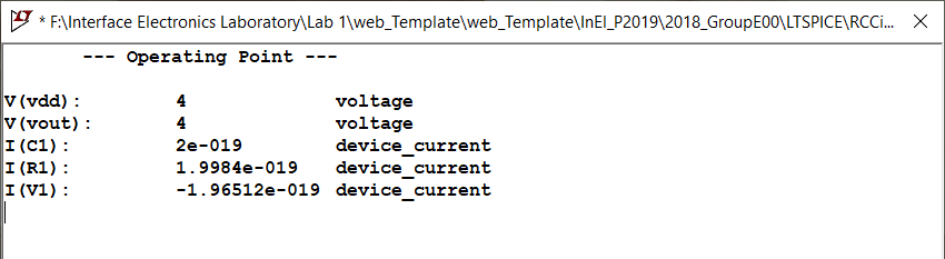
RC Circuit .op result
|
The result of this analysis is table of values, which correspond to the values of DC steady-state analysis, treating the capacitances as an open circuit. The values obtained are reasonable, in order that for the DC analysis, the voltage should be the same at the output. A value for the current was obtained, however it is too small that is practically considered to be zero. |
|
RC Circuit .tran result
|
The result of this analysis is a graphic in which the behaviour of the circuit could be observed in the time domain. As the name of the analysis, with this option the transient behaviour of the circuir could be observed. As expected for the circuit, as the input is a sinusoidal wave, the output has the same property. Taking into account that this circuit is a low-pass filter, is reasonable that to a frequency of 10kHz the output is attenuated. This is beacuse the bandwidth of the filter is defined as: \( F_c = \frac{1}{2 \pi {R} {C}} = 31.8 {Hz} \) which is a value much lower than 10 kHz |
|
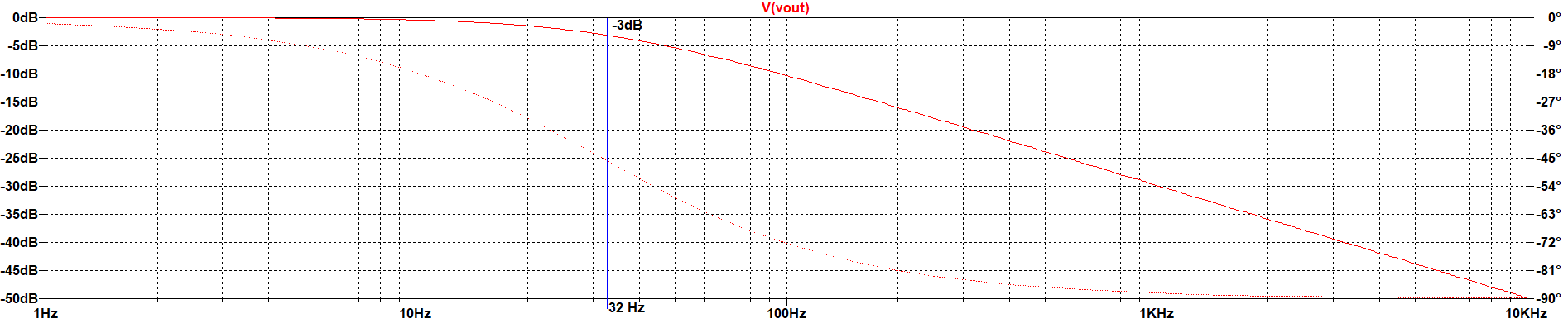
RC Circuit .ac result
|
This analysis allow us to make the small signal analysis over the DC operating point. As inputs, the selection of the limits to the frequency sweep are available. In the result, it can be seen that the output is the bode plot for the circuit at the band defined in the analysis. For the specific circuit, the frequency edge is almost 32 Hz by the formula. It can be seen that this number is nearly the value of -3dB magnitude |
|
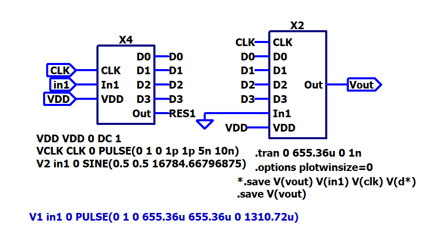
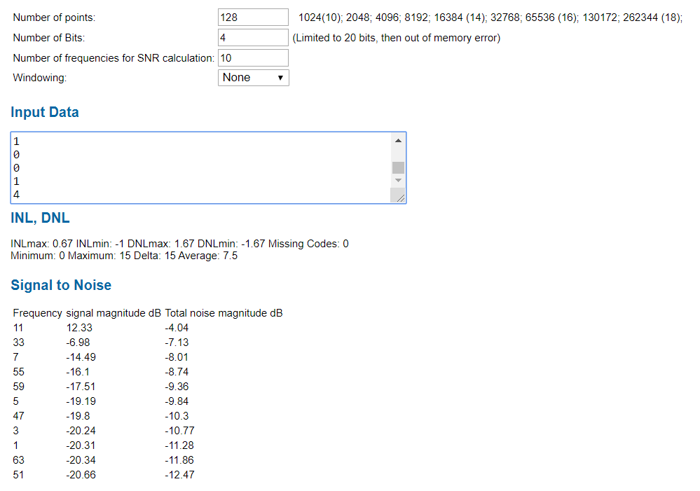
Ideal ADC and DAC converters
|
Following the instructions to build the schematic shown in the image, simulations were held from a sine and ramp input, in order to obtain data and measure the DNL and INL values |
|
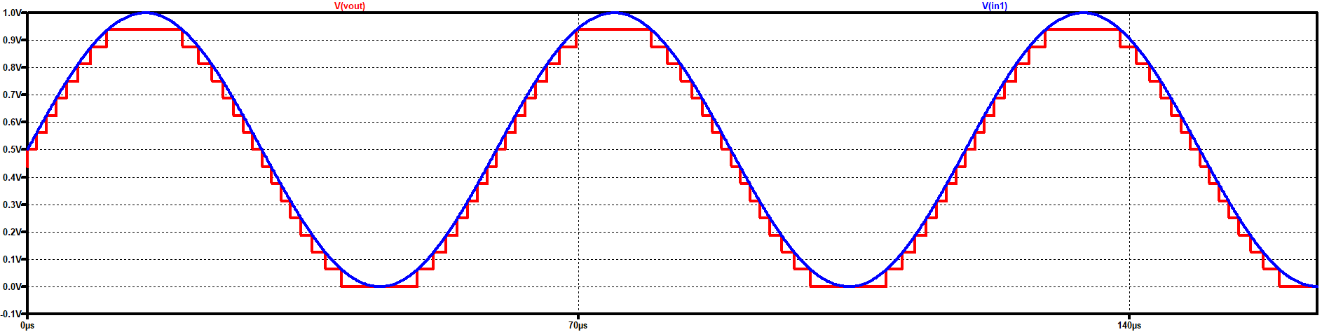
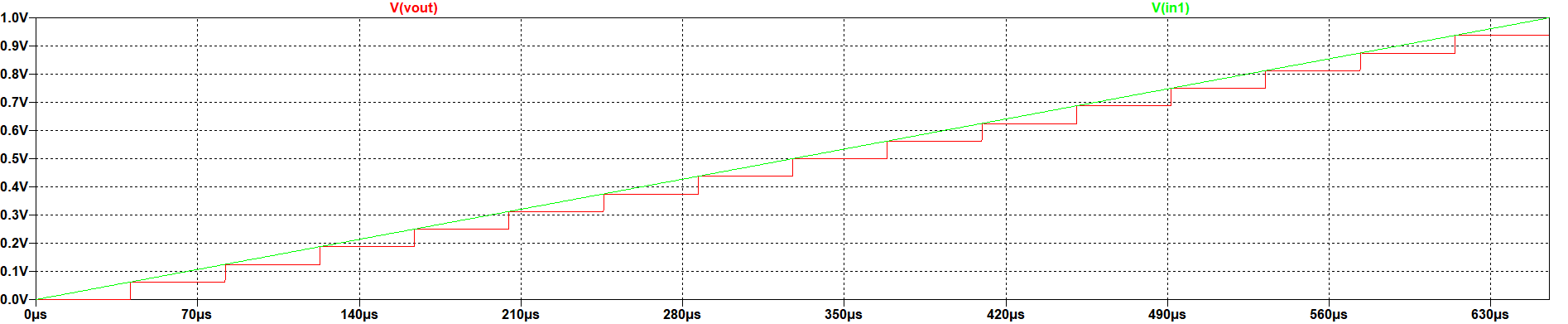
Ideal ADC and DAC converters
Sine wave input
|
The figure shows that the converter is following the form of the sine wave, but with fixed steps as it is an output based on fixed values. As the converter is 4 bit, the steps are 16. It can also be seen that the maximum output voltage is not the reference voltage, instead a voltage below 950 mV. The LSB can be calculated easily with the following formula: \( LSB = \frac{V_ref}{2^{N}} = 1/16 = 62.5{mV} \) and therefore, the maximum output voltage is: \( V_{out,max} = {LSB} \times ({2^{N}-1}) = 937{mV} \times 15 = 937{mV} \) |
|
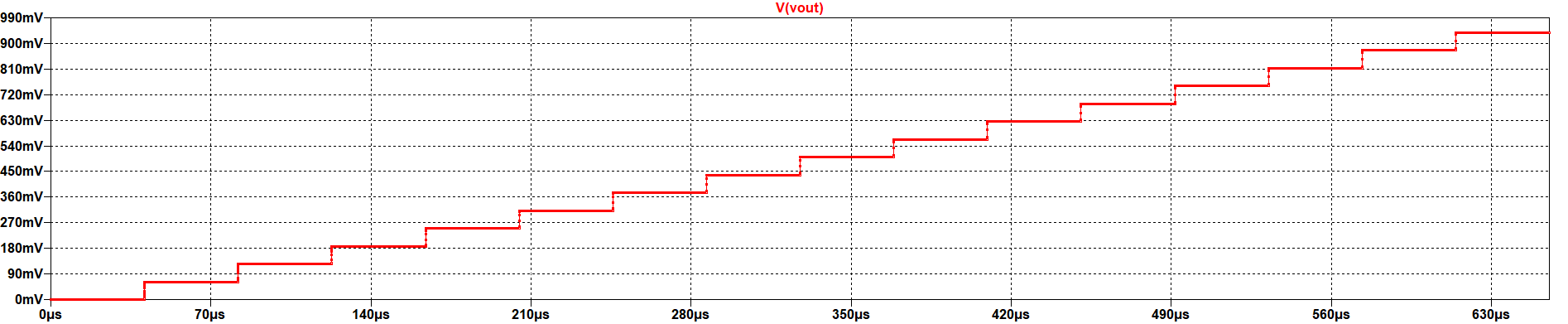
Ideal ADC and DAC converters
Ramp wave input
|
The figure shows that the converter is following the form of the ramp wave, but with fixed steps as it is an output based on fixed values. As the converter is 4 bit, the steps are 16. The calculations are also valid for this signal: \( LSB = \frac{V_ref}{2^{N}} = 1/16 = 62.5{mV} \) and therefore, the maximum output voltage is: \( V_{out,max} = {LSB} \times ({2^{N}-1}) = 937{mV} \times 15 = 937{mV} \) |
|
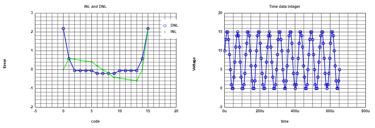
Ideal ADC and DAC converters
Sine wave ADC - DNL and INL
|
The figure shows the graphics of ADC - DNL and INL from the data of the simulation. That are the typical curves for DNL and INL for a sine wave using the histogram test. |
|
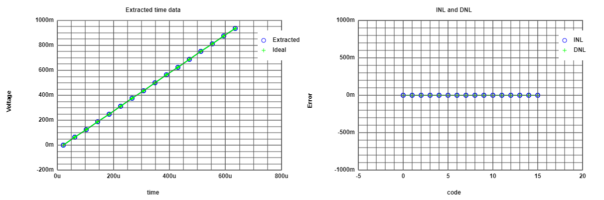
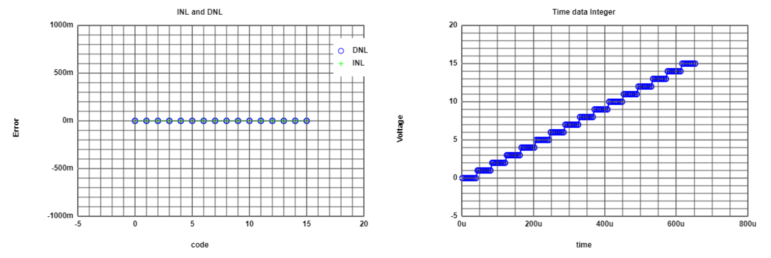
Ideal ADC and DAC converters
Ramp wave DAC - DNL and INL
|
The figure shows the graphics of DAC - DNL and INL from the data of the simulation. Here there is no error between the real and expected values, and therefore the DNL and INL are zero for all codes. |
|
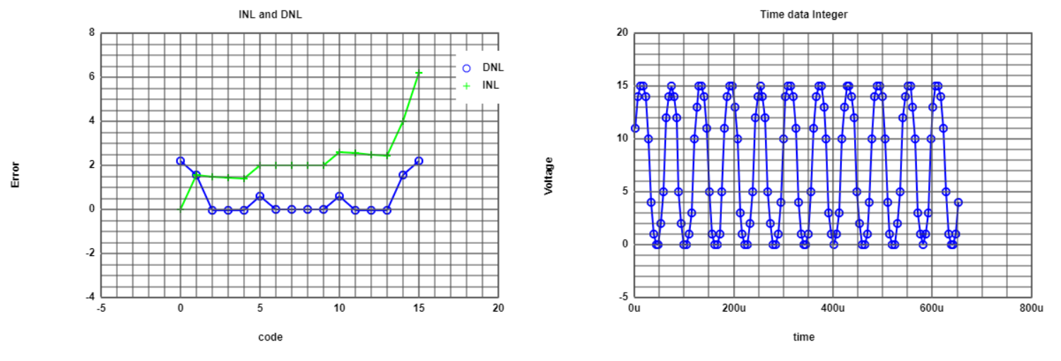
Ideal ADC and DAC converters
Ramp wave ADC - DNL and INL
|
The figure shows the graphics of ADC - DNL and INL from the data of the simulation. As the input is a ramp wave, and all the codes in the histogram have the same amount of samples, there is no error, and therefore no DNL and INL |
|
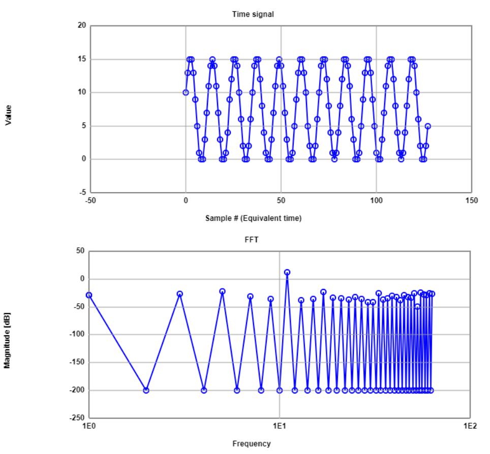
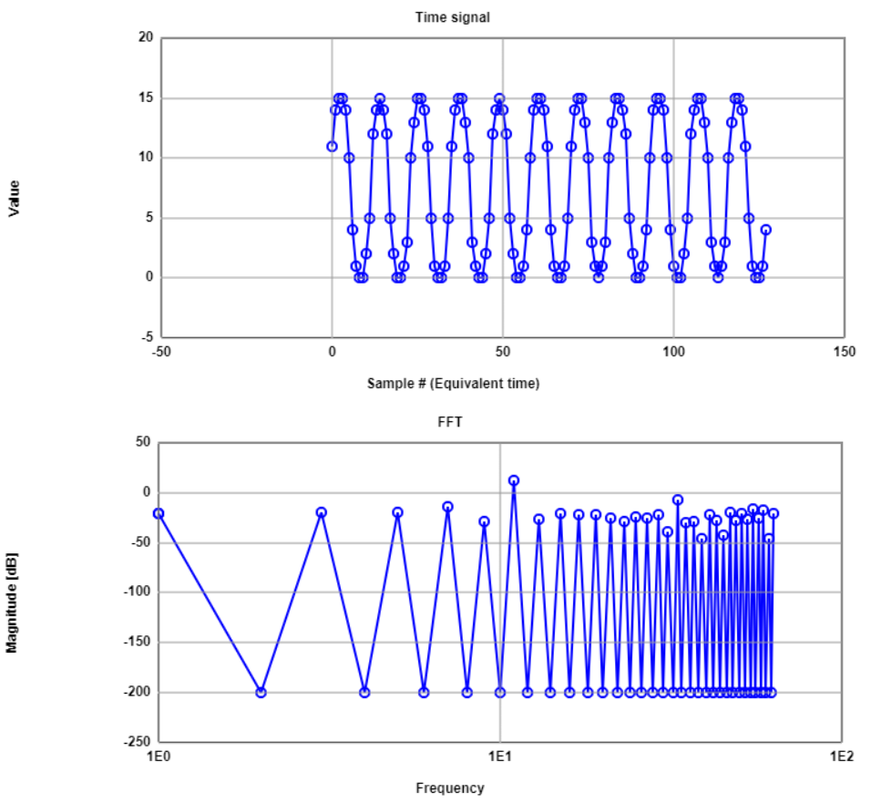
Ideal ADC and DAC converters
Sine wave FFT
|
The figure shows the FFT of the sine wave. There can be seen a peak at frequency 11. There are also some components of high frequency, but most of it could be considered the average noise magnitude. |
|
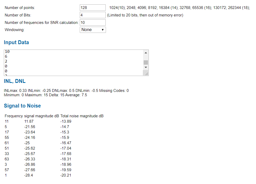
Ideal ADC and DAC converters
Sine wave SNR
|
The figure shows the magnitude of the sine wave FFT components. The principal component is located at frequency 11, and from there there is a margin of 25dB. |
|
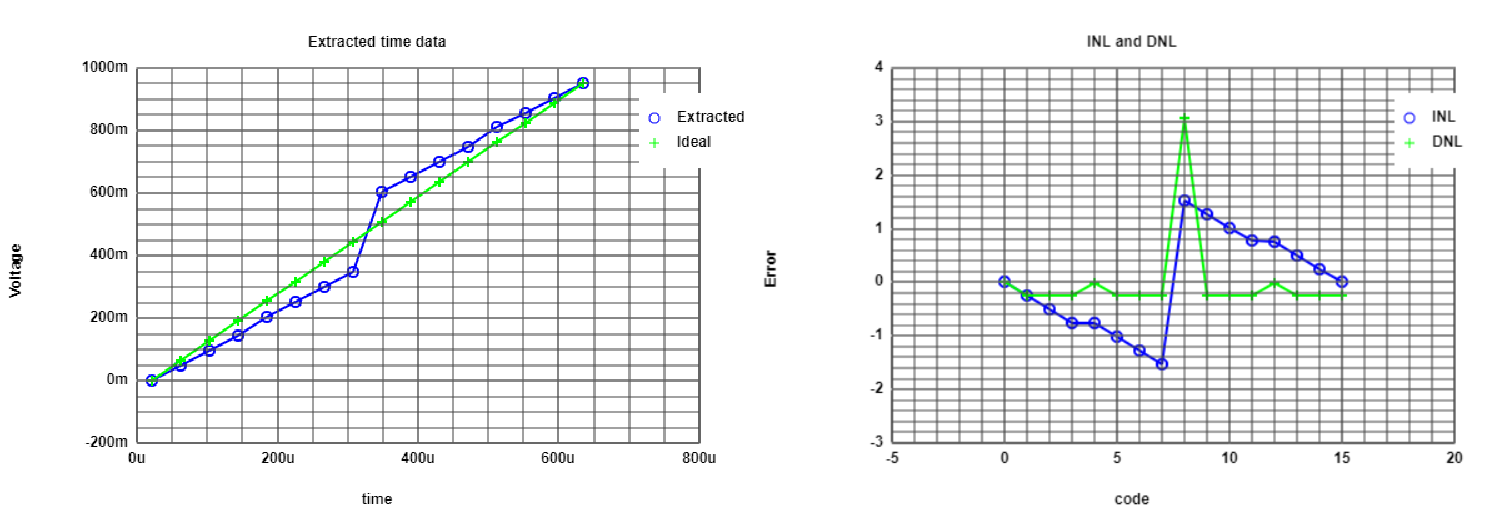
Ideal ADC and R2R DAC converters
R2R DAC - DNL and INL converter simulation
|
The following DNL and INL graphics is the response to the ramp wave. As expected, there is a change in the output characteristic, as the output values are not longer equilibrated to LSB steps, due to the change in the resistor values divisor are not set to the same ratio. |
|
Ideal ADC and R2R DAC converters
R2R ADC - DNL and INL converter simulation
|
The following DNL and INL graphics is the response to the sine wave. The DNL has almost the same behaviour as in the ideal case. But there are to peaks for 2 codes in the middle. The INL is icreasing as the DNL has no negative values. |
|
Ideal ADC and R2R DAC converters
R2R ADC - FFT
|
The following FFT graphics is the response to the sine wave. In real time, it can be seen that codes for middle values is nearly inexistent, but for the non-linear part of the sine, there are codes which are close to each other. The FFT of the signal looks very similar to the ideal one.Exists the same peak frequency, but the harmonics are more distinguishable. |
|
Ideal ADC and R2R DAC converters
R2R ADC - SNR
|
The figure shows the magnitude of the signal and the harmonics. According to this data, now the SNR is about 16.33 dB, which is considerably less than the ideal case. However, there is no lost of bits in this case |
|