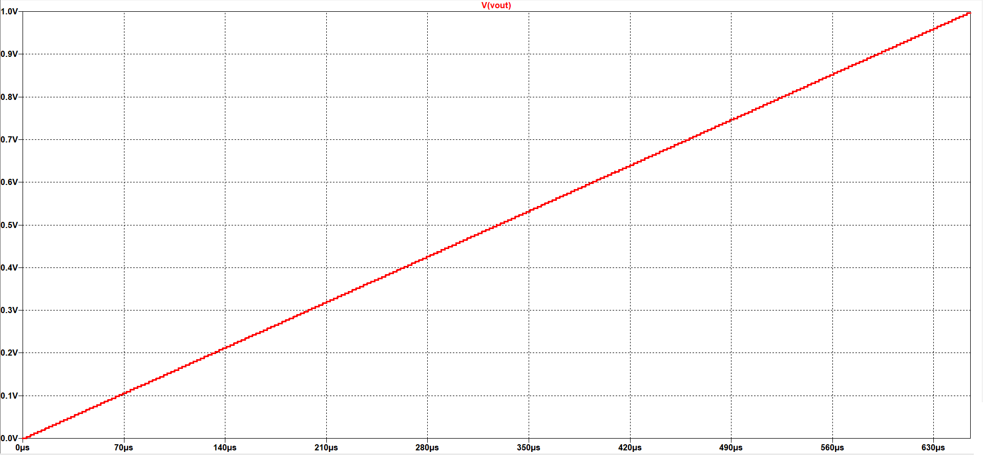
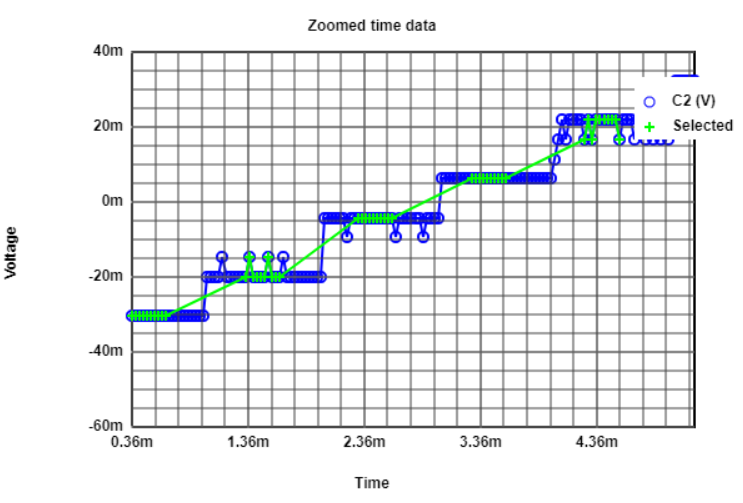
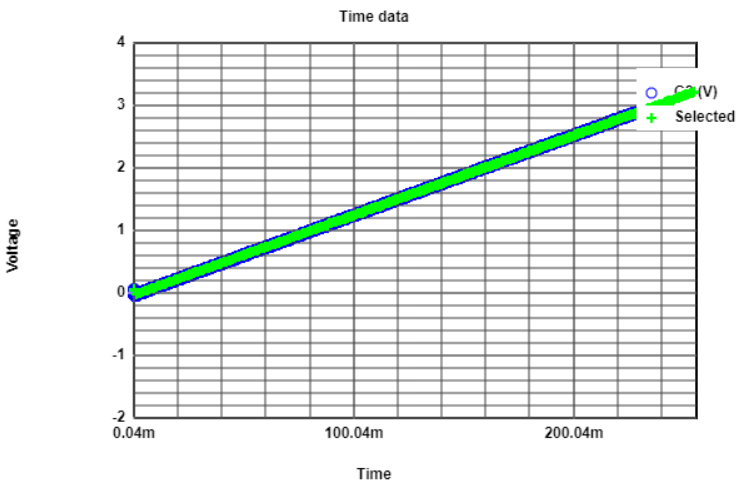
RampWave Output Result
|
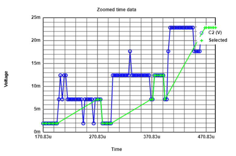
The image shows the result of a ramp wave input. It can be seen the discretization levels of the ramp wave over the time. As the converter has 8 bits, therefore the number of available code are as follows: \( {CODES} = {2^{N}} = 2^{8} = 256 \) The LSB can be calculated from the following formula: \( LSB = \frac{V_ref}{2^{N}} = \frac{1{V}}{256}= 390.6{µ V} \) and therefore, the maximum output voltage is: \( V_{out,max} = {LSB} \times ({2^{N}-1}) \) \( = 390.6{µ V} \times 255 ≈ 996.1{mV} \) |
|
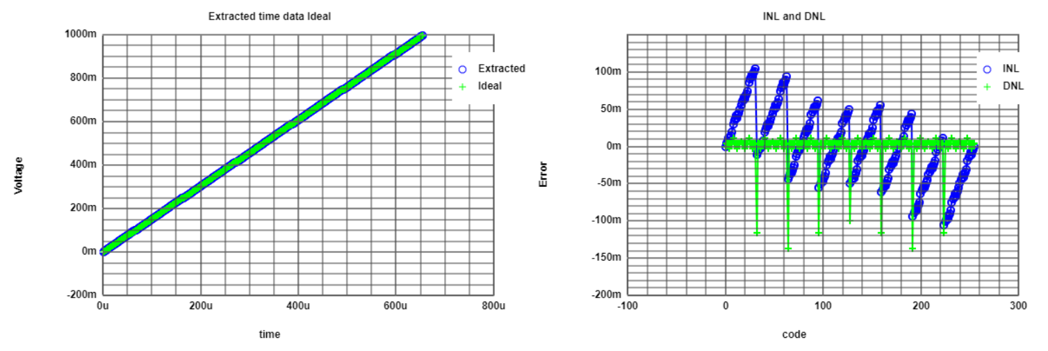
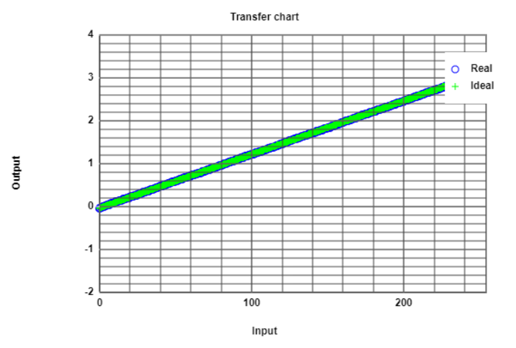
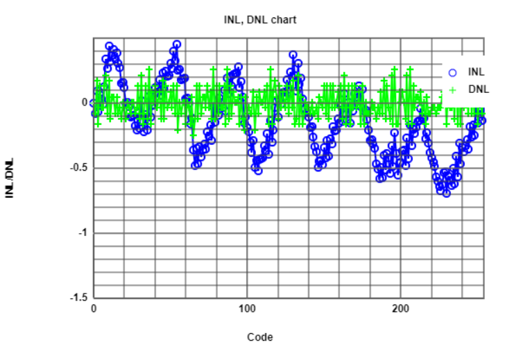
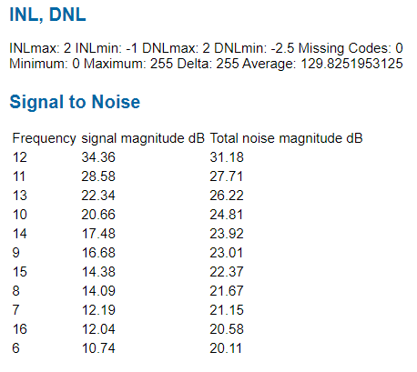
RampWave INL and DNL analysis
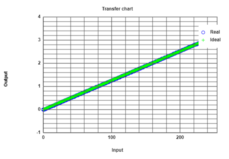
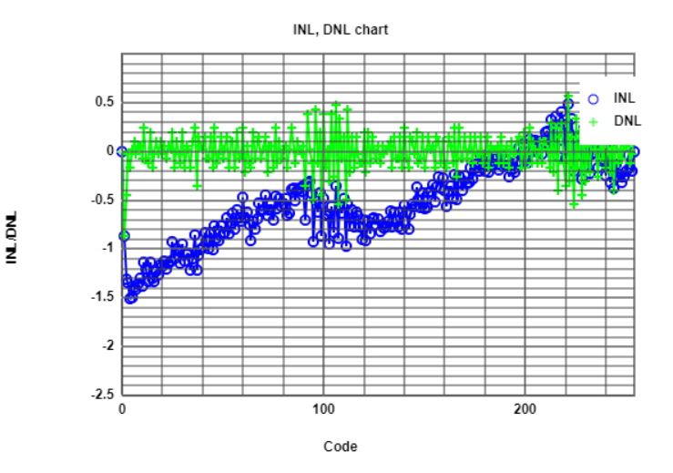
The following image is a result of the processed data by the Raw Data Analysis.
It shows the DNL and INL graphics for the rampwave.
It can be seen that the extracted and the ideal curve are nearly the same. However
there is a small DNL error which can be seen clearly in the accumulation ramp of the
INL, and periodically, there is big error in the DNL which changes the offset of the
INL ramp. Additionally, the magnitude of the error is quite small, and for a real
measurement perhaps accurate instruments are required. Here it can be seen the effect
of the uncompensated values of the resistances.
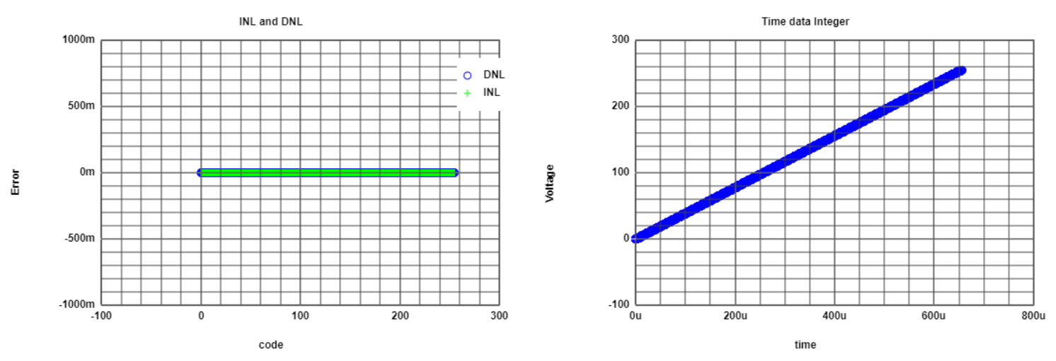
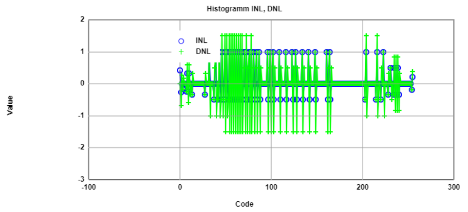
RampWave Histogram analysis
The following image shows the DNL and INL error for the histogram analysis. As the
number of occurrences is the same for all the codes, theoretically there is no DNL
error, which implies no INL error as well.
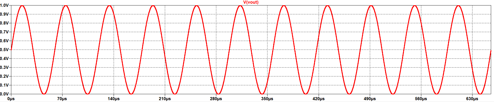
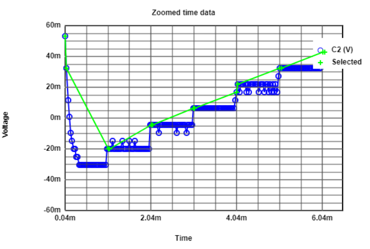
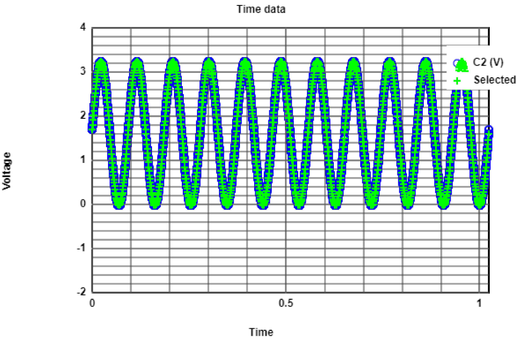
SineWave Output Result
The image shows the result of a sine wave input. It can not be
seen the discretization levels of the sine wave over the time,as
it seem a continuous signal, but with a zoom into it, the discretization
levels can be seen.
SineWave Histogram analysis
The following image shows the DNL and INL error for the histogram analysis. The
number of occurrences of the codes is not equally distributed, because the sine wave
has more samples at the peaks of the wave (non-linear function). These peaks are mostly
represented by the codes 0 and 255, and the DNL is proportional to the number of
measurements for each code. That is also the reason that for the codes for the linear
region of the sine wave, the error is minimum (codes 127 - 128).
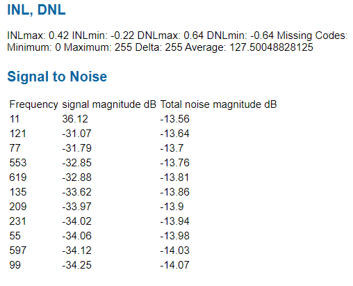
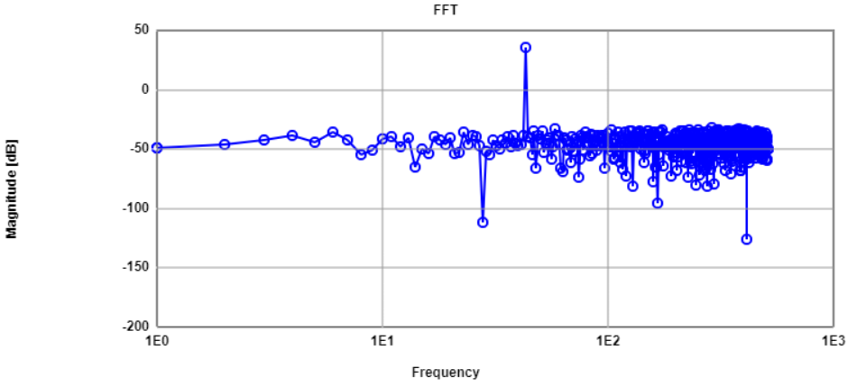
SineWave FFT analysis
The figure shows the FFT analysis for the sine wave. The number of points choosen for
the FFT was 4096. The amplitude of the voltage is 0.5 V, Offset 0.5 V, 11 periods.
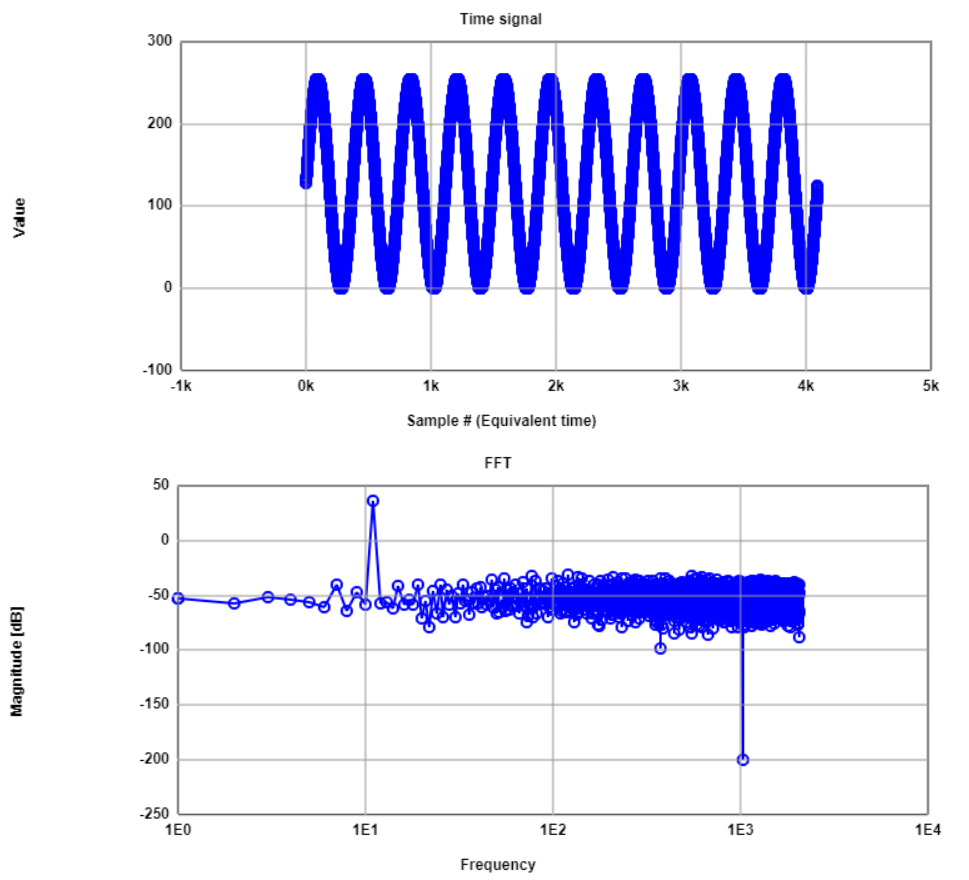
SineWave FFT analysis
The previous theoretical data seems to match with the FFT graphic, as well as the
SNR results presented in the following image:
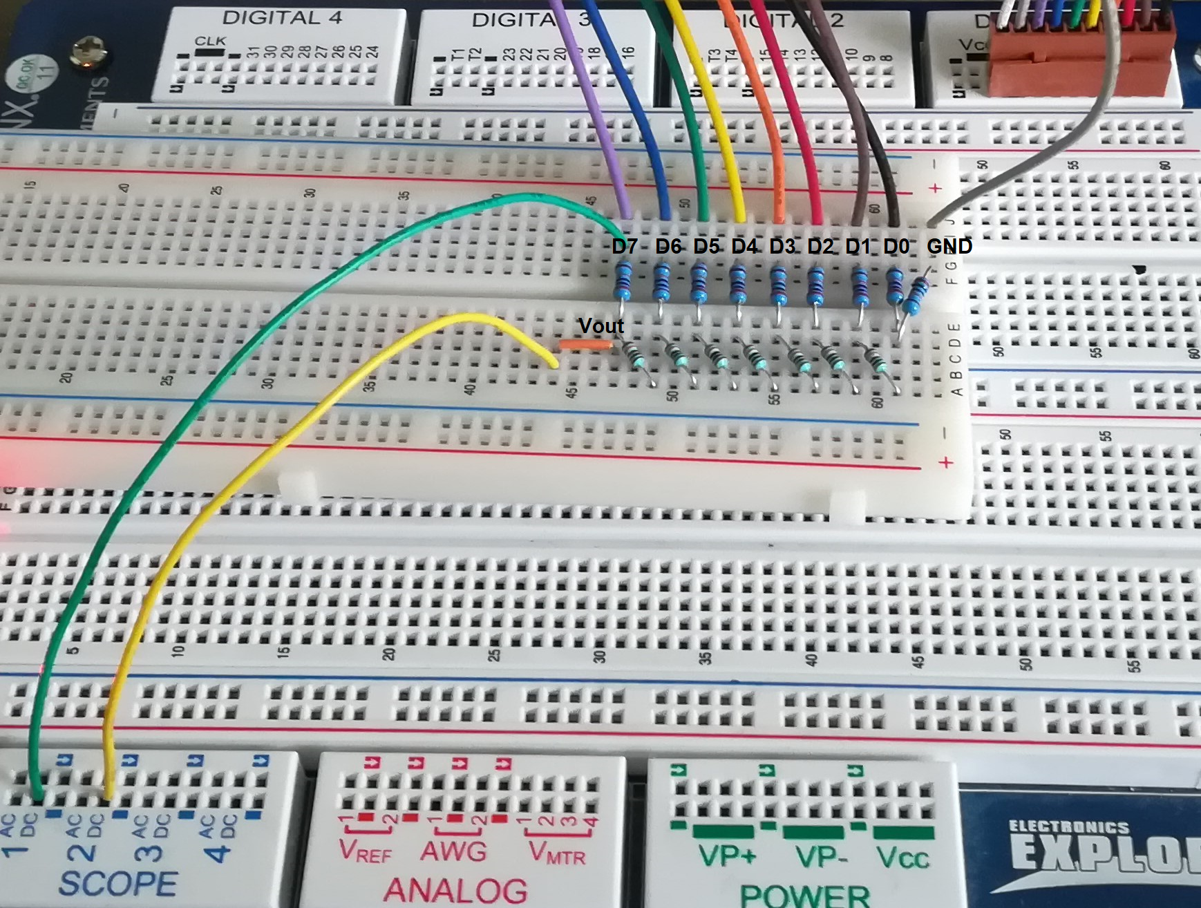
Real 8-bit DAC Circuit
Now, from the previous schematic, the R2R DAC structure was implemented on bread board.
The following image shows the physical distribution of the circuit and the conection between Electronic Explorer.
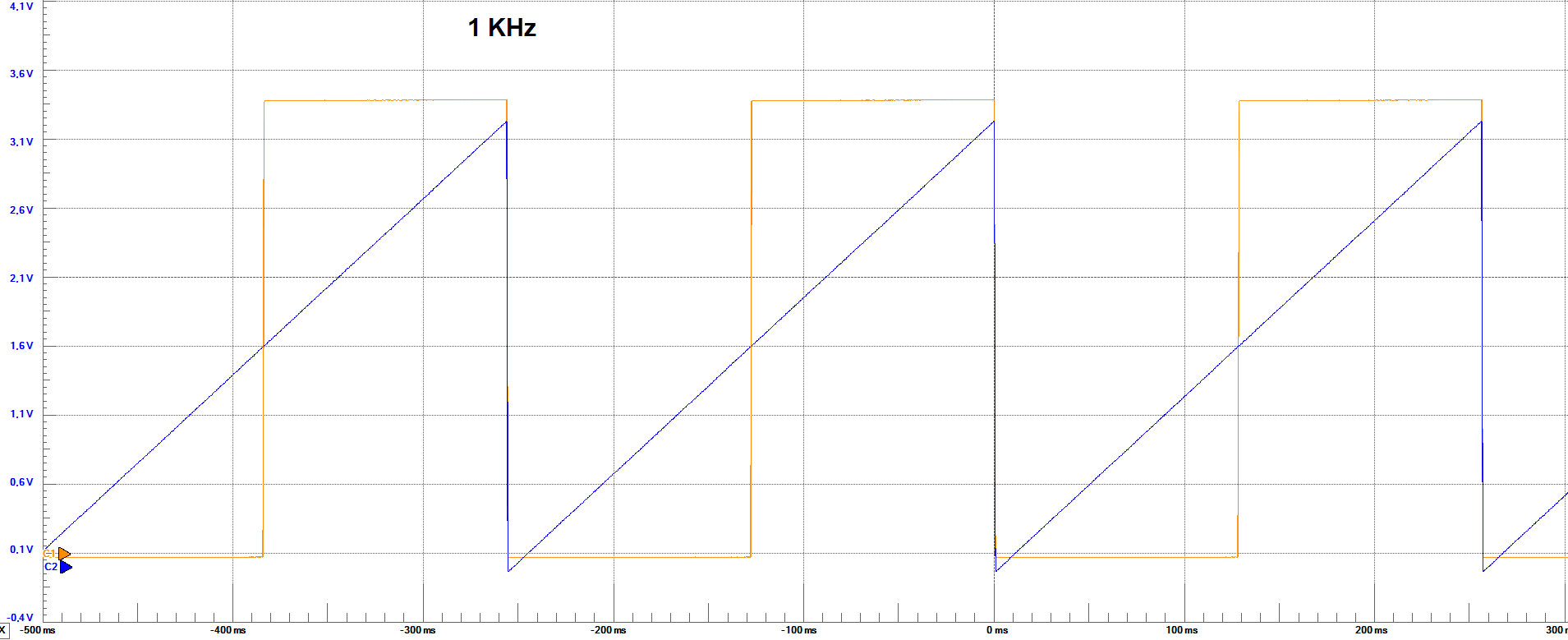
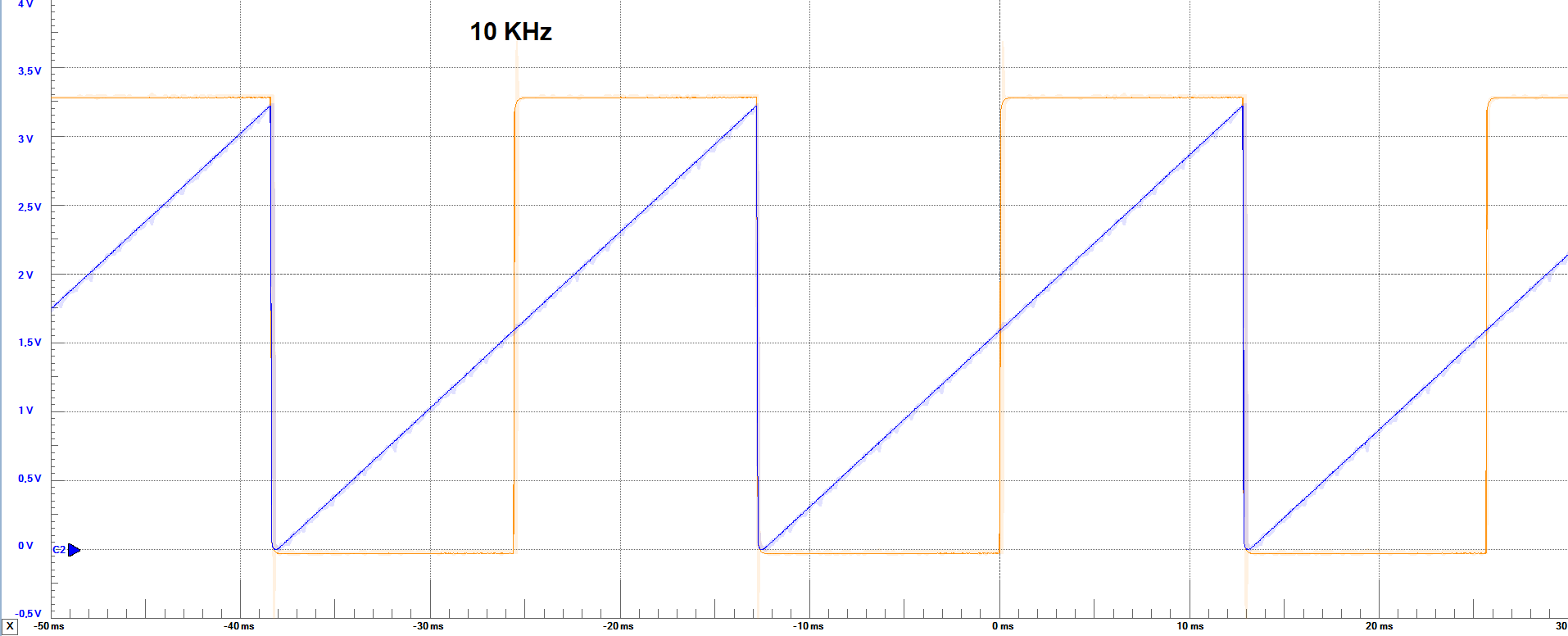
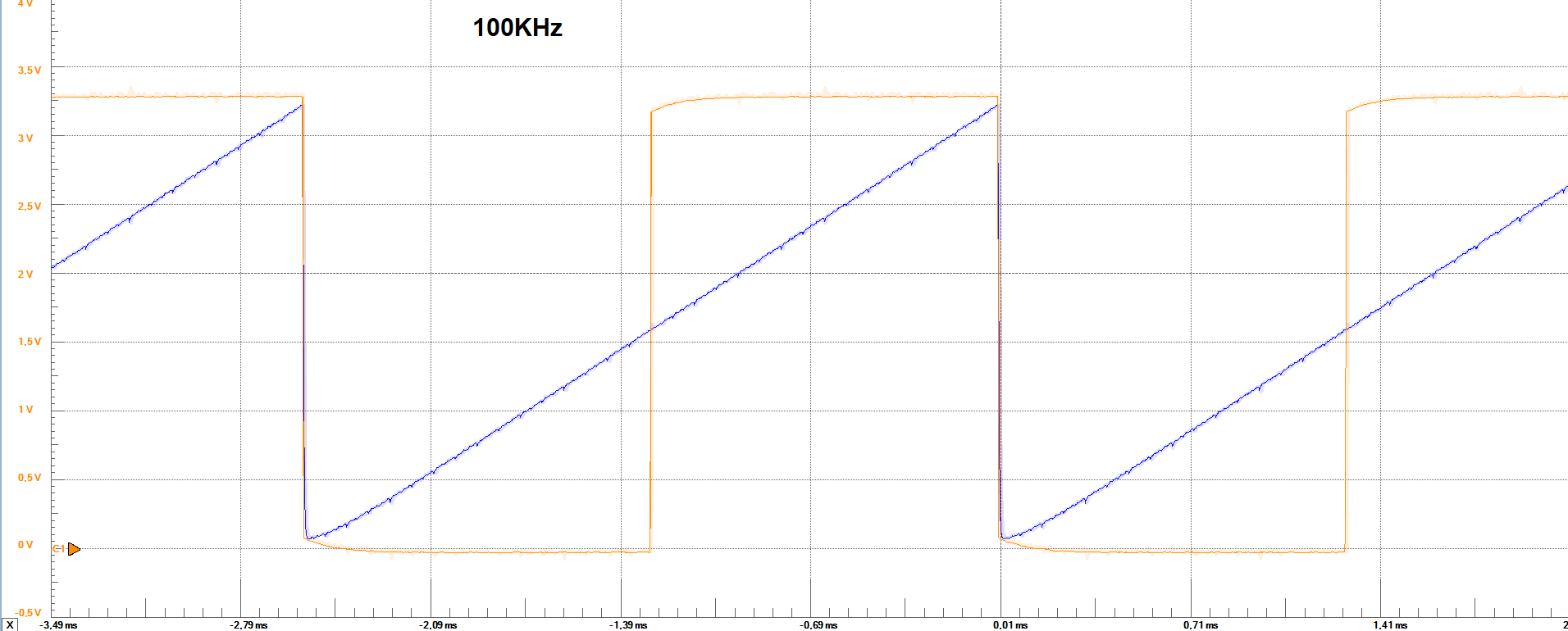
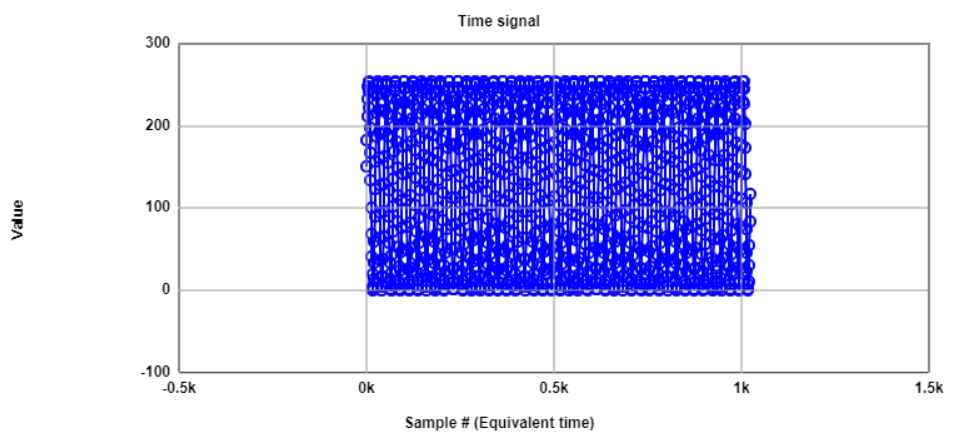
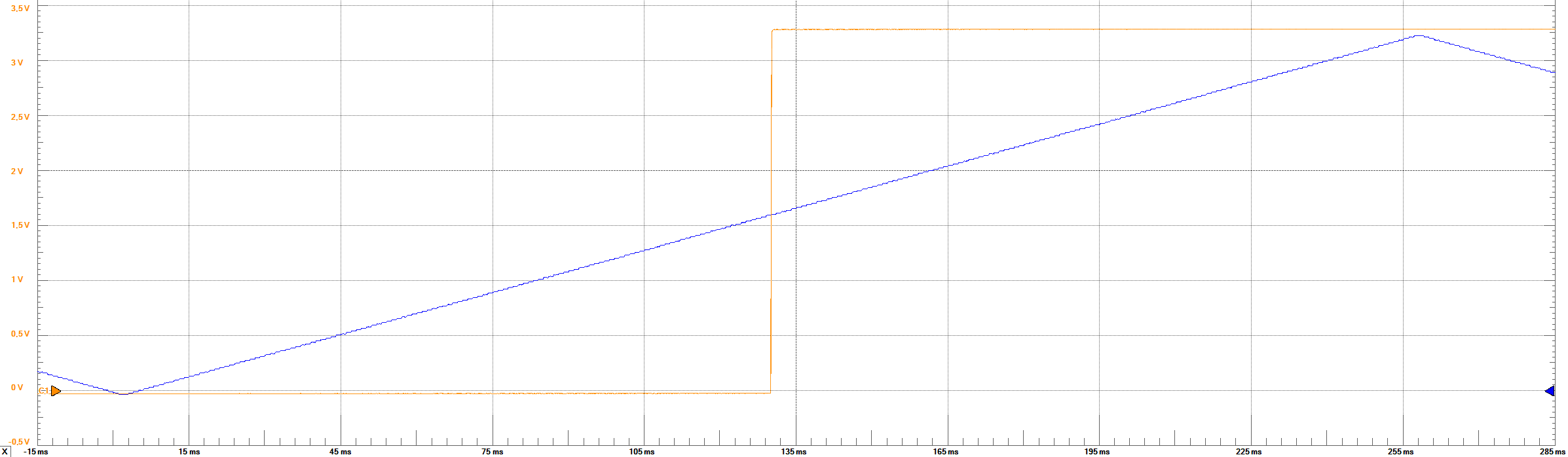
Measurements
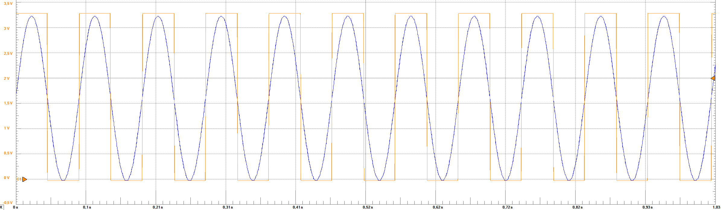
Output waveforms
The following images show the output wave form of the DAC - R2R, where for each image and for all in this document
the orange line represents the bit 8 of the converter (MSB), and the blue one represents the output analog voltage.
The frequencies were choosen acording to the instructions of the lab (1Khz, 10Khz, 100Khz),
the output frequency of the analog and also the MSB is not the same. I guess the selected parameter refers to the frequency
of the bit 1 of the converter (LSB).
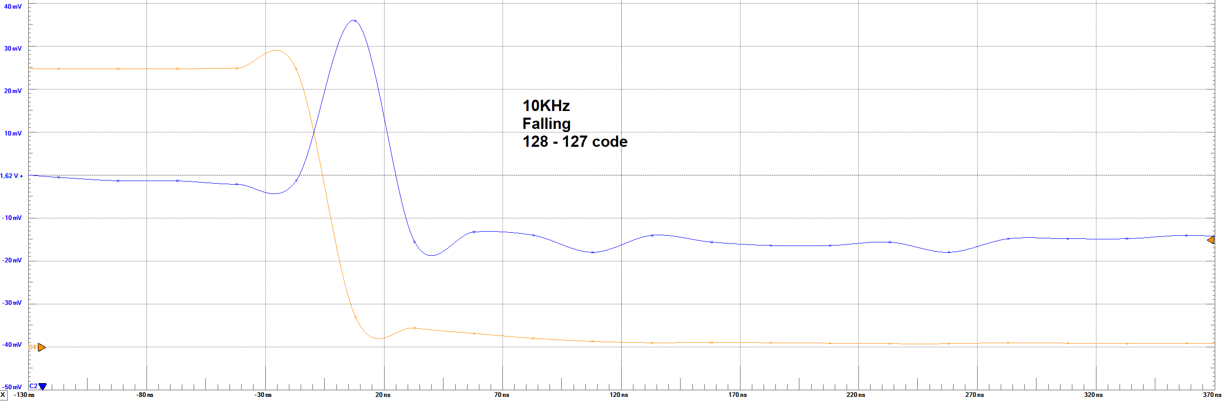
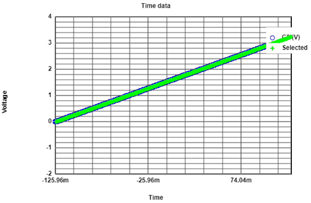
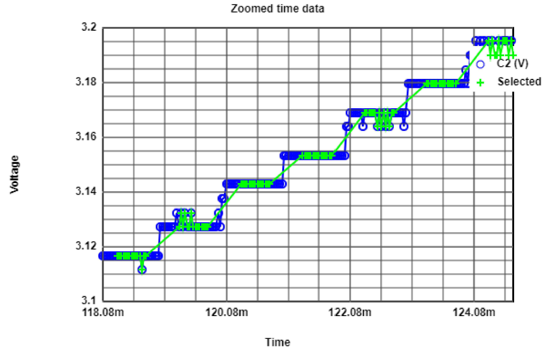
Measurements
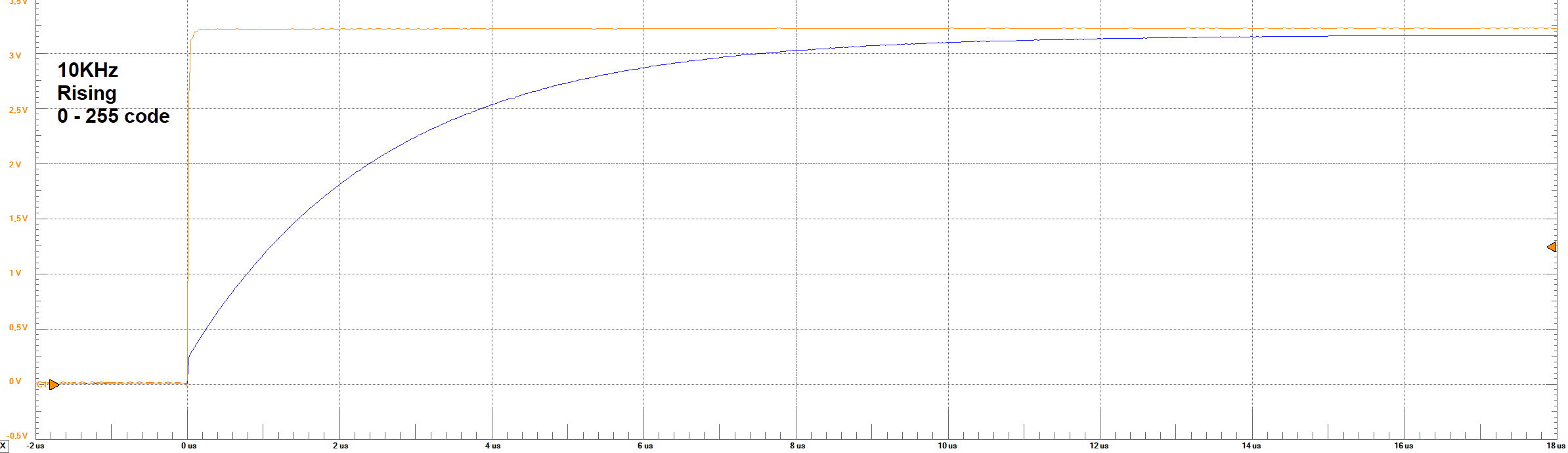
The following images show the outputwave form of the DAC - R2R with the goal to measure the settling times (falling and rising) by changing just 1 code step and full code step
The orange line represents the bit 8 of the converter (MSB), and the blue one represents the output analog voltage.
Settling Times - 10 KHz - 0 to 255 code step
Measurements
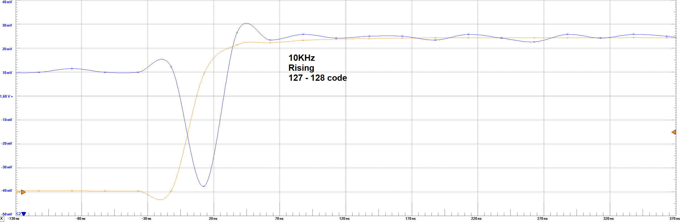
Settling Times - 10 KHz - 127 to 128 code step
The orange line represents the bit 8 of the converter (MSB), and the blue one represents the output analog voltage.
Measurements
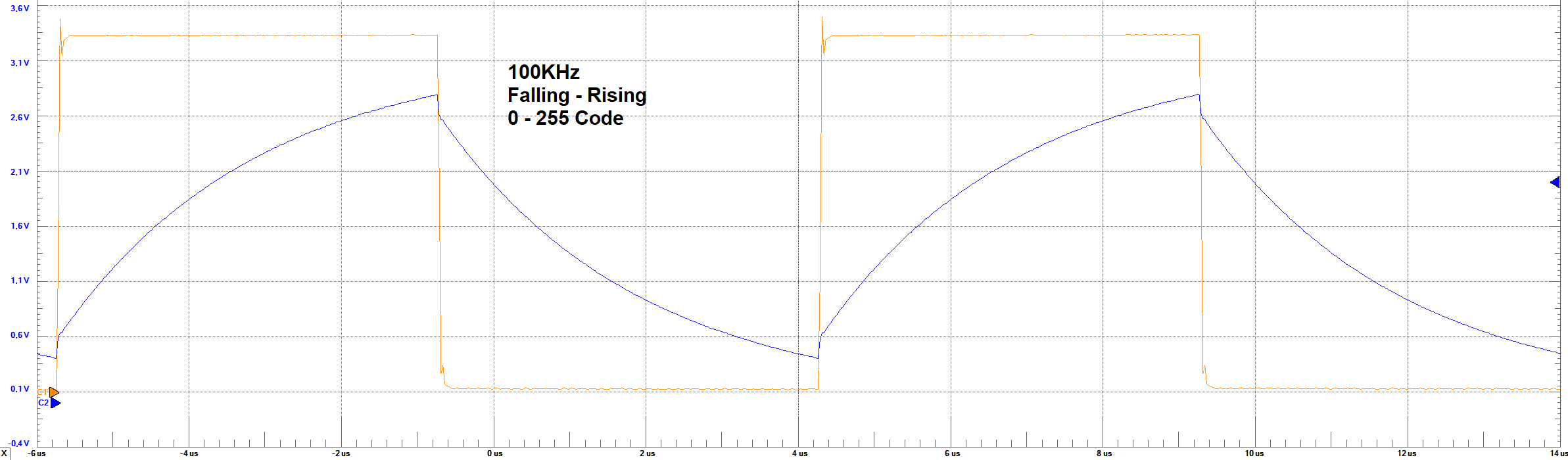
Settling Times - 100 KHz - 0 to 255 code step
The orange line represents the bit 8 of the converter (MSB), and the blue one represents the output analog voltage.
Measurements
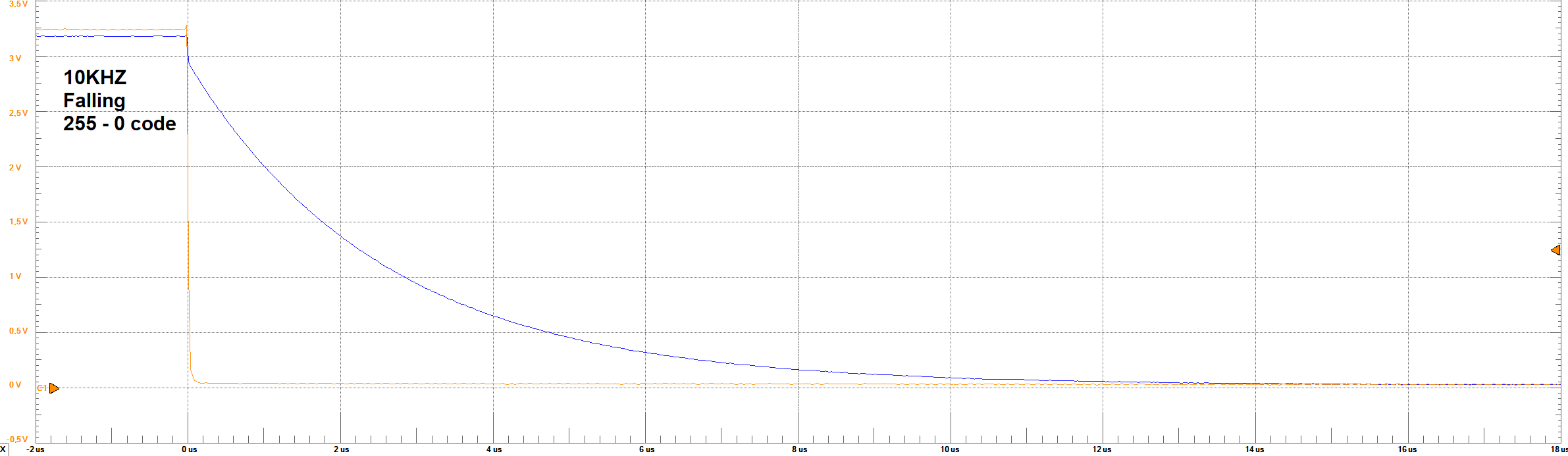
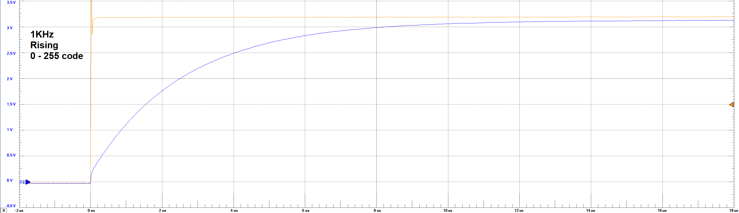
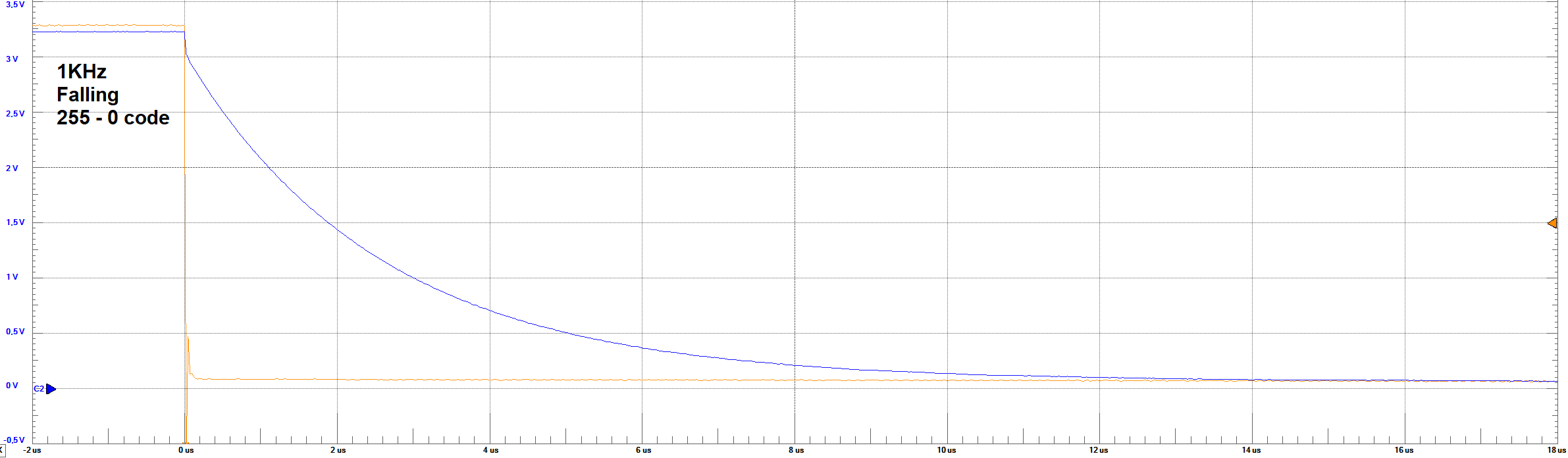
Settling Times - 1 KHz - 255 to 0 code step
The orange line represents the bit 8 of the converter (MSB), and the blue one represents the output analog voltage.
Measurements
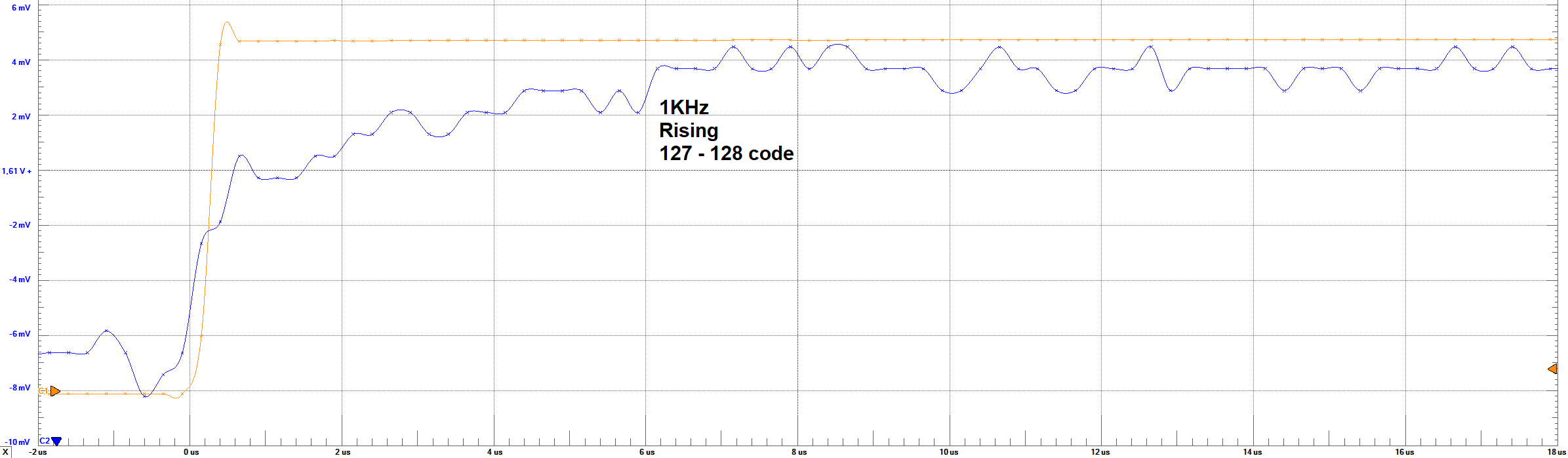
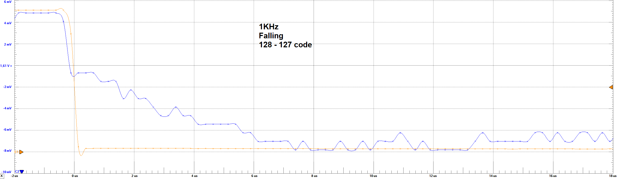
Settling Times - 1 KHz - 127 to 128 code step
The orange line represents the bit 8 of the converter (MSB), and the blue one represents the output analog voltage.
Measurements
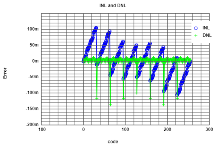
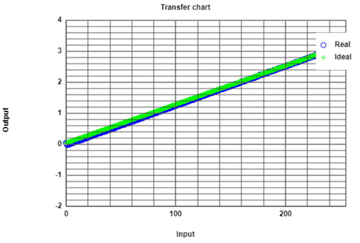
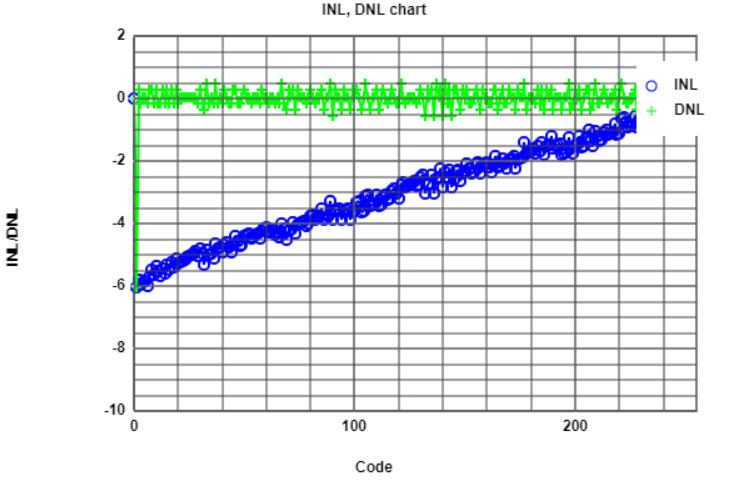
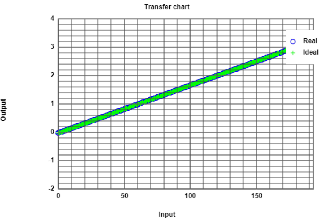
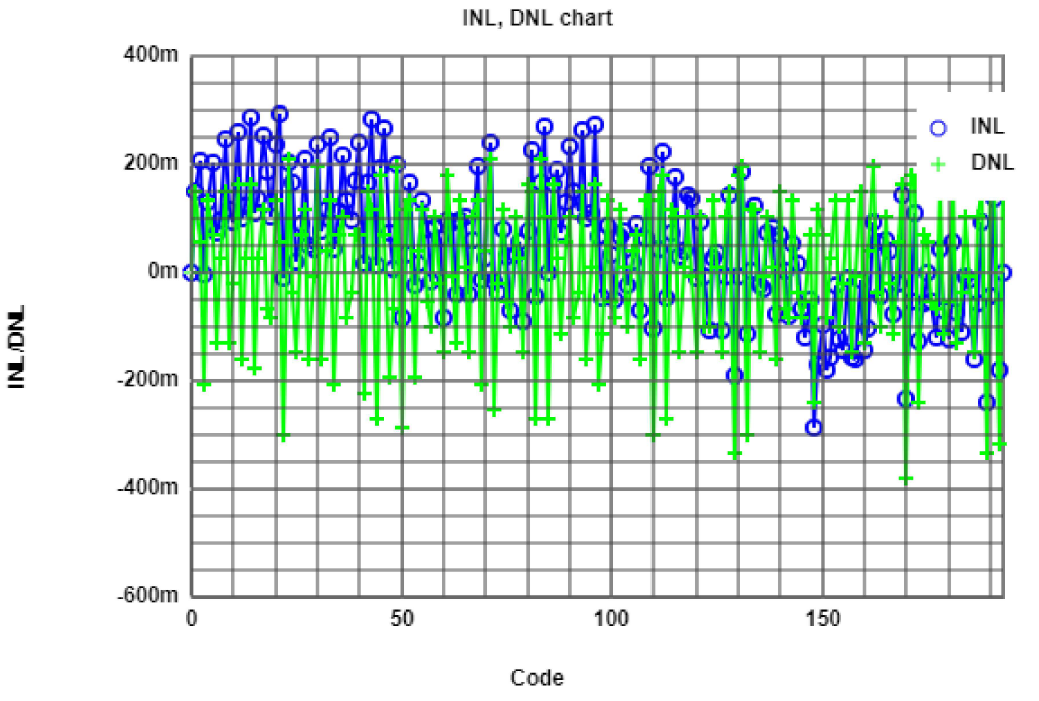
DNL and INL
Following the procedure, the filtered data of a rampwave was introduced to the Data Osc Procesor. From that tool, we can obtain (with apropiated selection of settings) the DNL and INL graphics.
10KHz Parameter
Results for the 10KHz binary output setting. 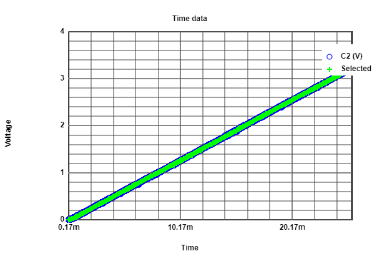 |
 |
 |
 |
Measurements
DNL and INL
10KHz Parameter Analysis
Aparently, the transfer chart give us the idea that the behaviour of the ramp is really close to the ideal ramp. However, the zoom area to the origin showed us that the data
points were not so stable for low codes. Also, the INL indicated that at low codes there was a huge amount of error, and for codes grater than 150 the errors are not so big.
As the INL is greater than 1 LSB, is not acceptable performance. the assumption that the parameter of 10KHz was still high enough was made, as for high frequency the output
deformed the ramp at low codes. Perhaps that was happening in this case, but was not observable. The subsequent step was to decrease the frequency parameter (for example: 1KHz).
1KHz Parameter
Results for the 1KHz binary output setting. 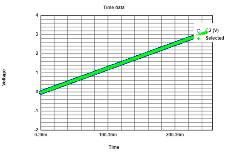 |
 |
 |
 |
Measurements
DNL and INL
1KHz Parameter Analysis
Now the INL and DNL have an acceptable range of error between +/-0.5 LSB, and the samples are better distributed into the steps. It can also be observed some noise over the
samples, but not considerable to damage the performance. The zoom window show also that the lowest codes have negative values, which mean that the minimum voltage is not 0,
and therefore could be an offset-error of -30mV.
Comparing also the DNL and INL graphic with the simulated circuit with the corresponding measured values of resistances, the shape of the waves are very similar,
so it was somehow expected.
Comparison between the measurement and simulated DNL and INL. Left(Measurement) and Right(Simulation)
| |
 |
With this behaviour, we can say that the problem here was due to frequency limits rather than the inaccuracy of the resistances. Even with 1% tolerance values, we get values
of INL and DNL between the desired range of +/-0.5 LSB. Therefore is not necesary to improve the circuit by changing resistances.
According to these results, the best frequency operation of the pattern generator is the lowest of the provided set. In this case, I had to do an extra measurement in 1KHz
in order to achieve error results between the desirable range.
Measurements
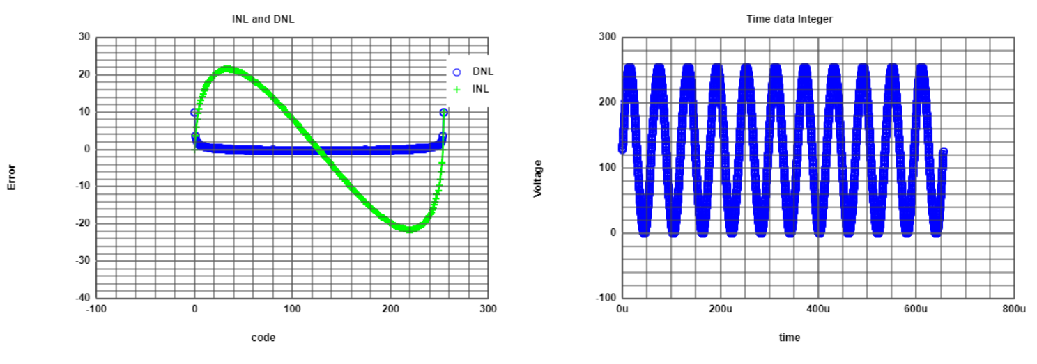
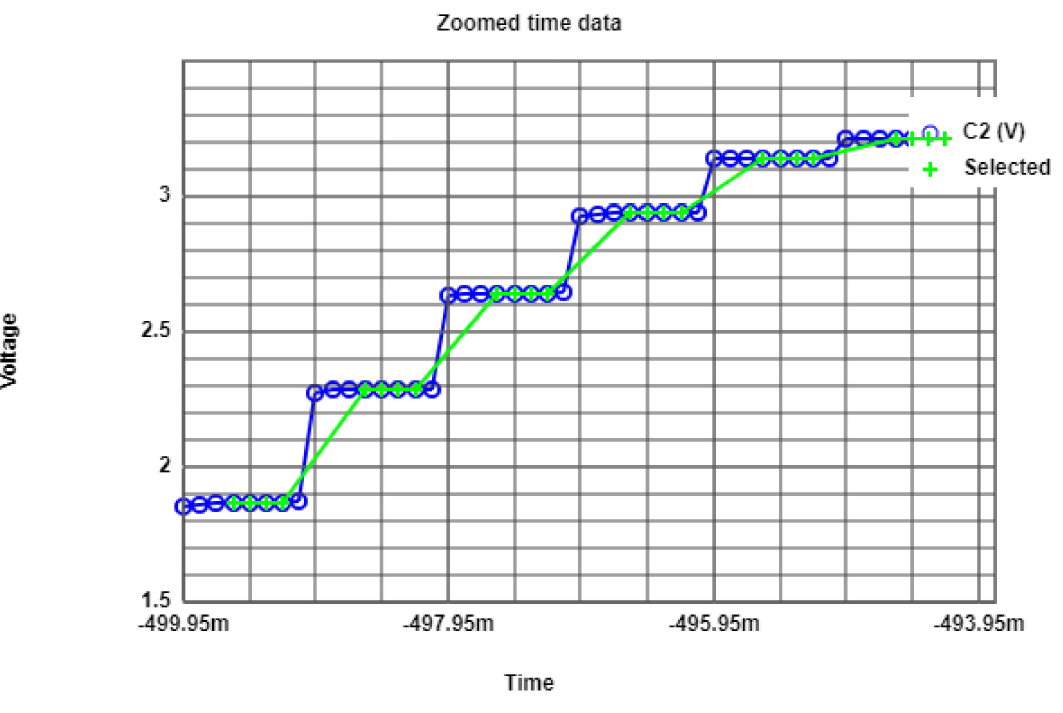
Bad extraction of rampwave
For the following example, a bad filtering of the data from a rampwave signal was given to the tool. Also, a bad selection of parameters in the tool was selected.
 |
 |
 |
 |
This was the same data used for the 1KHz analysis. As it can be seen, the wrong filtering of the data, specially on the edges of the rampwave,
summed also with a bad selection of data points for analysis, led to high values of error in DNL and INL graphic. Without knowing that the
input data is bad filtered, would lead to think that the converter has a gain error. A good filtering of the same data, lead to the results for
the 1KHz analysis. There a better performance over the DNL and INL error was obtained.
Measurements
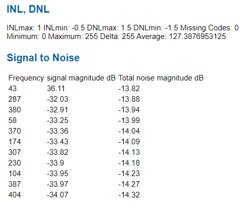
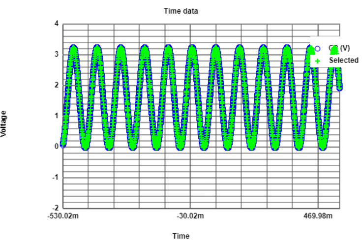
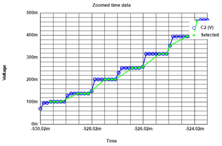
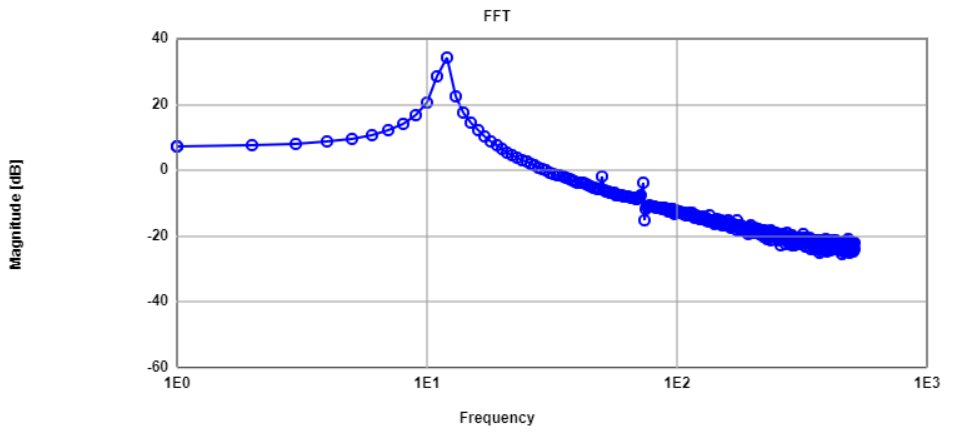
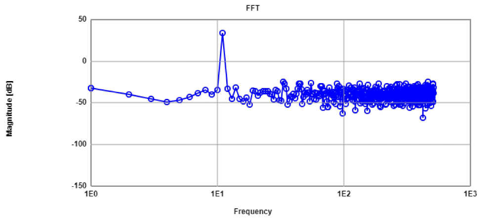
Sine wave input
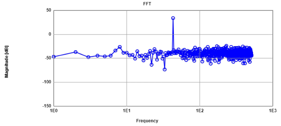
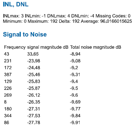
43 Periods SineWave
The file of the digital input of the sine wave was imported to the pattern generator as stated in the instructions.
The following is the FFT calculated from the FFT analysis tool. Before this tool was used, first the data needed to be converted from voltage into codes, in order to use the FFT tool.
Results shows the following information:
 |
 |
 |
 |
Measurements
Sine wave input
Bad Filtering example
For the following example, a sinewave with 11cycles was introduced to the circuit and the output was measured. The data was converted into integers, so the
FFT analysis could be done. the following is the result of bad data filtering.
 |
 |
 |
 |
From the time data it can be seen that the wave has more than the requiered 11 periods of the signal. For that reason the selected data is not equally distributed over
the range of the codes. The FFT result shows that rather than a pure sine signal, it is more like a sum of harmonics and frequencies near the real frequency. The solution
for this data is to fit the correct data points to form 11 cycles of the signal.
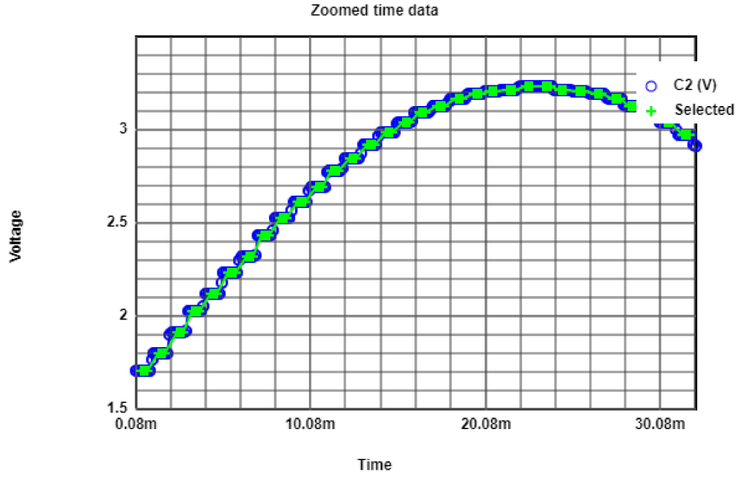
Measurements
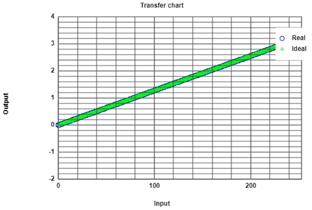
Calibration ramp input
For the calibration process, a ramp wave input is introduced to the circuit. The output is measured to generate a lookup table to give better performance in the
INL and DNL parameters of the converter.
Th following image presents the output to the rampwave input.
 |
Measurements
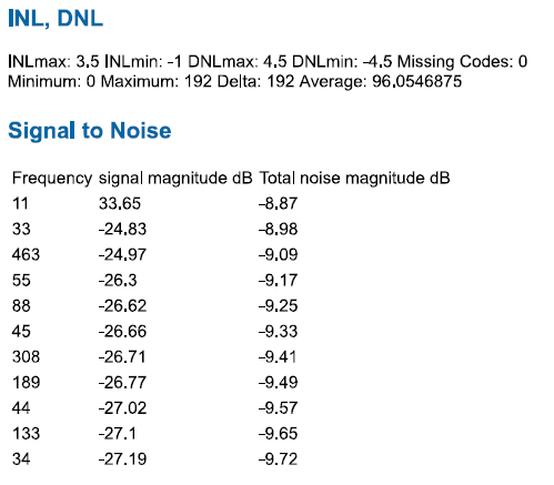
Calibration Lookup Table
The analysis given by the tool for the rampwave is the following:
 |
 |
 |
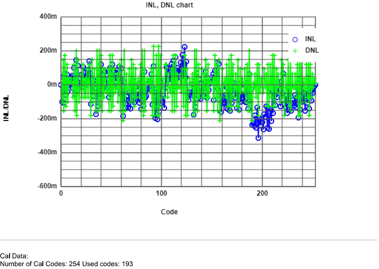 |
It can be seen that the DNL and INL error magnitude is within +/- 0.5. Using the tool to obtain the calibration codes, it gave
that for the new ramp, 193 codes will be used. These codes were copied into the ramp generation with calibration and
obtained a file that was fed into the pattern generator.
Measurements
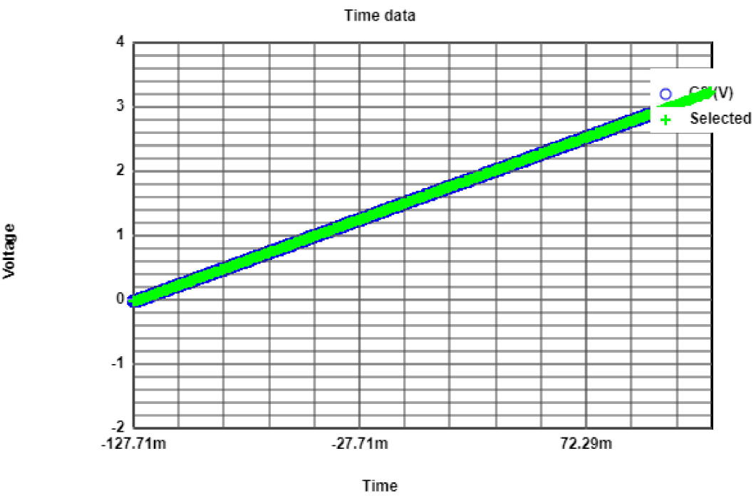
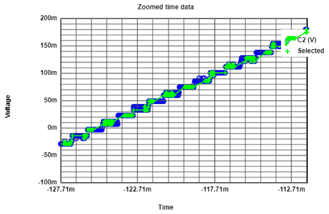
Calibration Results
Again a ramp wave was obtained and measured. From the DNL and INL graphic, the codes used in this new ramp are less.
Also, it can not be seen a subtancial improvement in the error magnitude, and in fact it seems that the number of peaks in the error graphic
are more than without calibration.
The analysis of this ramp is the following:
 |
 |
 |
 |
Measurements
Calibration Results
Using the same lookup table, a sine wave of 11 cycles was used. The following images shows the output, the reading process of the data and the FFT
 |
 |
 |
 |
Measurements
Calibration Results
Using the same lookup table, a sine wave of 43 cycles was used. The following images shows the reading process of the data and the FFT
 |
 |
 |
 |