R2R DAC LTSPICE Simulation
 |
The schematic shows a 4-bit R2R DAC.
Build the circuit on a breadboard.
Measure the values of the resistors and document it in a table.
Build a 8-bit R2R DAC in LTSPICE with the measured resistance values.
Create a symbol and hook it up to the ADC DAC test circuit from last week.
Expand the test circuit like the slide "Test for 12 Bit ADC" in the presentation LTSPICE .
Simulate ramp and sine and extract INL, DNL and SNR data.
Simulate a ramp test.
Extract the simulated values with Read Raw File .
Calculate INL, DNL with any tool or use ReadOsci.html and paste the extracted values from LTSPICE into the input field.
Document and discuss INL and DNL values.
Simulate a sine signal test.
Extract the simulated values with Read Raw File .
Calculate FFT, INL, DNL with FFT webpage and paste the extracted values from LTSPICE into the input field.
Document and discuss FFT, INL, DNL and SNR values.
DAC measurement procedure
- Measure settling time: Full scale, mid scale
- Measure ramp
Extract oscilloscope data
Generate calibration data
Generate calibrated ramp - Measure calibrated ramp
Extract oscilloscope data - Generate sine data
Measure sine
Extract oscilloscope data
Analyze sine with FFT - Generate calibrated sine data
Measure sine
Extract oscilloscope data
Analyze sine with FFT
Define in the digital pattern generator one more channel for oscilloscope trigger.
Full scale: Define in the pattern generator a PP (push pull) clock
Mid scale: Put MSB on a separate channel as PP clock with 180° phase difference.
This gives you a mid scale 011111..100000 pattern.
For waveform generation DDS (direct digital synthesis) web page is used.
Fill in the number of bits. Push button "Generate a default calibration" table.
The number of points should be 4 times the number of used codes.

At the bottom of the page the EE vector data can be found.
A ramp up and down minimizes settling time issues.
Background for the need to extract data from oscilloscope data is given lecture: DAC practical considerations
Settling time
Full scale: Define in the pattern generator a PP (push pull) clock
Mid scale: Put MSB on a separate channel as PP clock with 180° phase difference.
This gives you a mid scale 011111..100000 pattern.
Ramp generation
For waveform generation DDS (direct digital synthesis) web page is used.
Fill in the number of bits. Push button "Generate a default calibration" table.
The number of points should be 4 times the number of used codes.
At the bottom of the page the EE vector data can be found.
A ramp up and down minimizes settling time issues.
Data extraction and analysis
Background for the need to extract data from oscilloscope data is given lecture: DAC practical considerations
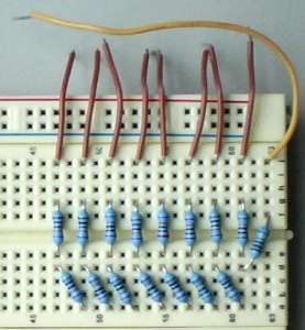
Breadboard R2R DAC
 |
Duration 14:27 min 2019_V04_R2R_DAC_ramp.mp4 |
Start the digital pattern generator and oscilloscope for a ramp measurement.
Extract INL and DNL.
Details:
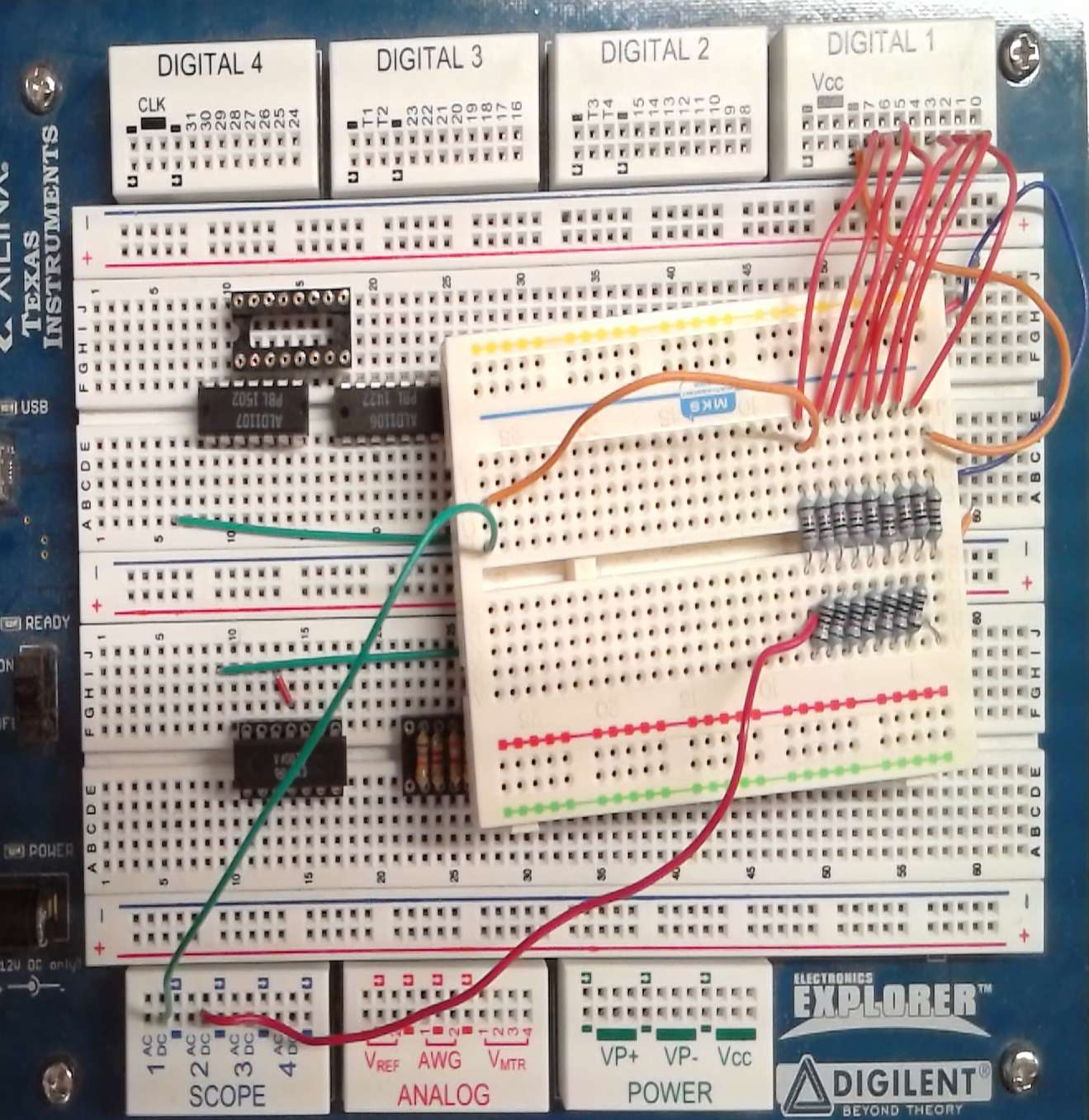
Data inputs are realized with DIGITAL1 0..7. All GND pins (Bold dash or small white arrow on colored background) are connected on the Electronic Explorer.
Connect D7 to SCOPE 1 DC input. This will be the trigger signal.
Connect Vout to SCOPE 2 DC input. This is the output of the DAC.
Make a photo of your setup connected to the Electronic Explorer.
Start Waveforms.
Start the oscilloscope: Scope
Start the digital Patterns
Select DI0..DI7 as bus and counter to generate a rising ramp
Generate a binary counter pattern with the pattern generator and look with the oscilloscope at the output of the 10-bit DAC.
- Measure the resistance values with a multi meter.
- What is the offset, maximum voltage, LSB and settling time of the DAC?
Measure the signal Vout.
Details:
Open the 'Patterns' window.
Create a bus with D[0]..D[7].
Use the type binary counter, output PP.
Select a frequency of 10 MHz, 1 MHz, 100 kHz, 10 kHz under 'parameter' for the counter.
Connect the MSB to SCOPE 1 DC as a trigger signal.
Connect the output of the DAC to SCOPE 2 DC and change the counter frequency until you have a sawtooth curve.
- Measure and extract INL and DNL using
ReadOsci.html
Details:
With the oscilloscope do export data.
Copy the data into the 'input data' field.
Make sure to measure a positive ramp.
Set 'DNL, INL start', 'DNL, INL averaging length', 'DNL, INL step' and 'DNL, INL number of values' to appropriate values.
Set option for measurement analysis to 'Ramp INL, DNL'.
Do 'Process oscilloscope data'.
Document and discuss the result.
Select a frequency of 10 MHz, 1 MHz, 100 kHz, 10 kHz under 'parameter' for the counter.
What is the best frequency for the pattern generator for operation?
Document challenges, effort and results and discuss your results.
2019.11.11: Added task:
Show results of good extracted ramp data versus bad extracted ramp data.
Discuss the difference.
- Select the best frequency from the previous task.
Can you improve the INL and DNL of the transfer characteristic by changing resistors?
Measure the improved circuit.
Document the improved resistance values.
Document challenges, effort and results and discuss your results.