Hochschule Kempten      
Fakultät Elektrotechnik      
Interface Electronics       Fachgebiet Elektronik, Prof. Vollrath      

Interface Electronics

Laboratory 01/02

GroupA05, ***456, G

ADC and DAC LTSPICE simulation


Overview

Installation of Webpage

Test of 4 Bit ADC and DAC

A 4 Bit ADC and DAC pipline can be simulated in LTSPICE.
The files were downloaded and the LTSPICE simulation was configured
The input voltage V1 is digitalized trough the X4 ADC. The X2 DAC will than take the digital signals and convert them back in to a continous-time discrete amplitude signal.
As voltage source a ramp from 0 to 1 V and a rise-time of 655 µs is used.

Simulation results 4 Bit ADC and DAC

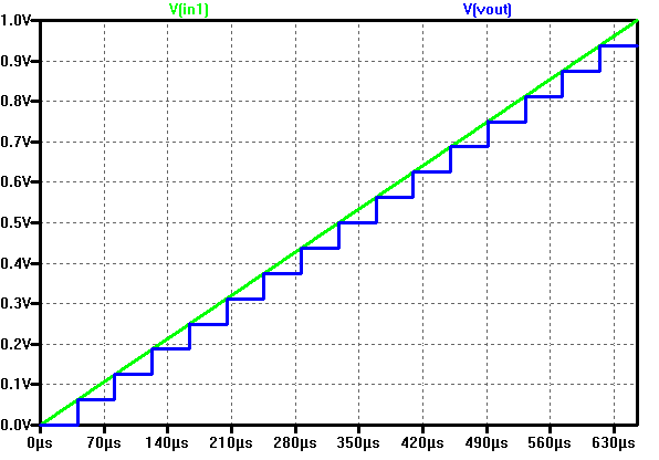
The picture shows a ramp input voltage and the DAC ramp output voltage over time.
In total 16 steps can be seen.
With a measurment statement the voltage levels were extracted:
.MEASURE V00 FIND V(Vout) AT=20us
At 60 µs the output of 0.0625 V is given for the code 01.
V01: V(Vout)=0.0625 at 6e-005 No error in the voltage level can be seen.
This shows that the ADC and DAC used here are ideal.

Test of a 3 Bit DAC

The schematic on the right represents a 3 Bit DAC.
One bit is represented by two square vawe signals having the same freqency but inverted logic levels.
So for three bits there are a total of six input signals. The LSB input signal level is toggled every 1 µs.
Therfore the MSB is toggled every 4 µs. This generates a binary count-up from 000 to 111 at the DAC input.
The resistors of the DAC do not have all the same values. So it is expected that the output voltage level steps will not be equal.

Simulation results of the 3 Bit DAC

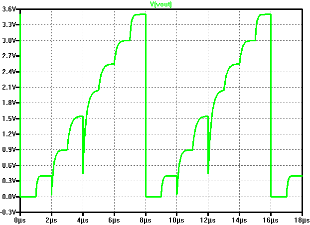
The picture on the right shows the DAC output voltage in function of the time.
It is clear to see that there is a small delay before a steady output voltage is reached.
This is due the RC elements in the circuit.
The output voltage level are measured just before each transition, by using the following spice directive:

.MEASURE V00 FIND V(Vout) AT=0.95us

3 Bit DAC transfer characteristic


Calculation of the LSB for the 3 Bit DAC:

Step size:     \( LSB = \frac{V(111) - V(000)}{2^{3}-1} = \frac{4 - 0}{7} = \frac{4}{7} V = 0.571 V \)

Ideal output voltage of DAC:

\( V_{ideal} = code * LSB \)

DAC Differential non linearity (DNL)


Calculation of the DNL for the 3 Bit DAC:

Step size:     \( LSB = \frac{V(111) - V(000)}{2^{3}-1} = \frac{4 - 0}{7} = \frac{4}{7} V = 0.571 V \)

The step size between 2 successive codes is normalized with LSB and calculated as DNL:

\( DNL(n) = \frac{ V(n) - V(n-1) - LSB}{LSB} \)

The graph and the table represent the same data and contain the same information.

DAC Integral non linearity (INL)


Calculation of the INL for the 3 Bit DAC:

Step size:     \( LSB = \frac{V(111) - V(000)}{2^{3}-1} = \frac{4 - 0}{7} = \frac{4}{7} V = 0.571 V \)

The difference between real and ideal curve is normalized with LSB and calculated as INL:

\( INL(n) = \frac{ V_{real}(n) - V_{ideal}(n-1)}{LSB} \)

The graph and the table represent the same data and contain the same information.

Summary


The 3 -bit DAC behaves in a realistic way.
From the transfer characteristic it is possible to see that there is a gain error in the output voltage.
Starting from the binary code 3, the error on the output voltage is well over the ±0.5LSB.
So, in conclusion the performance of the 3-bit DAC is poor.

The most challenging task in this laboratory was to generate the report in a HTML format.
I spent most of the time to change the JS function which generated the tables and corresponding graphs.

References


[1] Making of a Webreport , Vollrath

[2] Interface Electronics 03 Ideal ADC, DNL and INL , Vollrath