Simulation of a 4 bit ADC & DAC for a Sine signal
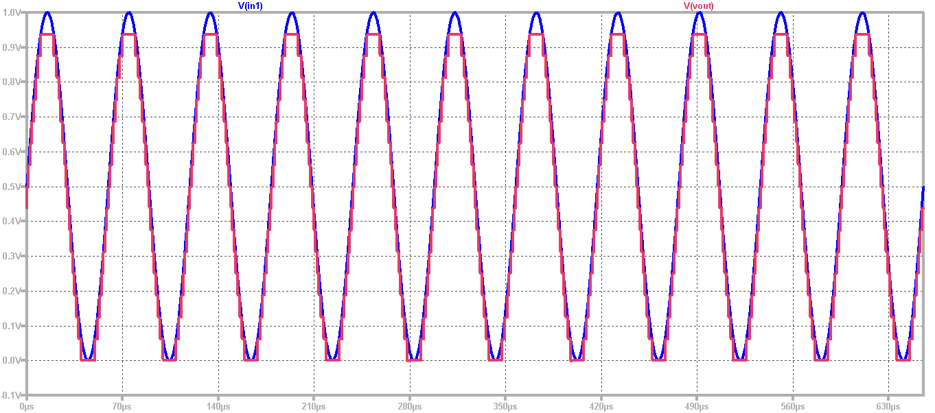
A Sine wave has been simulated for a 4 bit ADC and DAC with ideal components.
The output analogue wave can be seen in the red in the simulation given below.
A Sine wave with 11 periods can be seen in the figure given below.
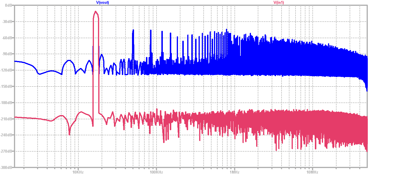
Fast Fourier Transform for a Sine signal
A Fast Fourier transform for a sine signal can be seen in the given figure.
The signal to noise levels has been observed and the input has better Signal to noise level because it is just a 4 bit converter.
We need external data processors because LTSPICE doesn't provide with all the values.
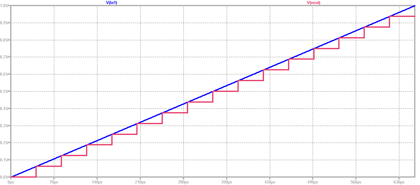
Schematic and Simulation of a 4 bit ADC & DAC for a Ramp signal
|
A Ramp response for a 4 Bit ADC and DAC has been observed in LTSPICE. A source has been added for this purpose. V1 in1 0 PULSE(0 1 0 655.36u 655.36u 0 1310.72u) |
 |
INL and DNL Analysis for a Ramp Signal
For Filteration, we have used an online Javascript tool.
The tool can be accessed using the Read Raw File given at the webpage of Lab 3 of Interface Electronics.
Then, raw.file was used for further analysis.

Histogram Test of ADC for a Ramp Signal
I got the results given below by again using the Javascript tool.
For this test, I increased the number of steps, in order to see how many times each digital code word appears on the output of ADC.
INL and DNL are zero because of the ideal case.

INL and DNL Analysis for a Sine Signal
I got the INL and DNL by again using the Javascript tool.
The graph on the left side shows the INL and DNL for the sine signal.
The graph on the right side shows the extracted values.

FFT Data Analysis for a Sine Signal
For a better analysis, I did the Fast Fourier Transform using the FFT webpage provided.
I also also observed the Signal to Noise Ratio (SNR).
The graph on the upper right corner shows the FFT for the Sine Signal.
The grpah on the lower right corner shows the histogram test.
 |
 |
 |
 |
Simulation and Analysis of R2R DAC for a Sine Signal
You can see the FFT for R2R DAC for a Sine Signal on the upper right side.
You can see the variations in INL and DNL and it is not ideal because we changed the resistance values.
The change of resistance values and corresponding INL/DNL values depicts that any minor change can be observed by having a look at INL and DNL graph.
 |
 |
 |
Simulation and Analysis of R2R DAC for a Ramp Signal
The INL and DNL graph can be seen at the right side of the figure given below.
The graph on the left side shows the effect of each individual change of resistance, the variation in the middle corresponds to change of R9 value.
The variation depends on the order of the bit.
 |