Microelectronics04 InverterProf. Dr. J÷rg Vollrath03 MOSFET |

|
Video of lecture 04 14.4.2021
|
Lõnge: 01:25:00 |
0:2:21 1um PFET 40 uA/V-2 0:5:30 RC Delay 0:7:0 Inverter 0:8:30 Transfer curve 0:15:48 Curve shift with width of NFET 0:23:23 Added of C 0:27:13 Switching of inverter 0:32:53 Add load and driver for delay measurement 0:41:13 Attach probe with R and C 0:42:50 Layout of standard cells and naming 0:51:33 List of rules and guidelines 0:52:16 Standard cell good example 0:55:23 Pass gate and transmission gate 0:58:16 NFET pass gate maximum voltage 1:1:3 Transfer gate 1:7:9 Pass gate simulation 1:12:53 Power consumption 1:17:43 Area per transistor |
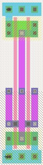
Inverter schematic and layout
|
|
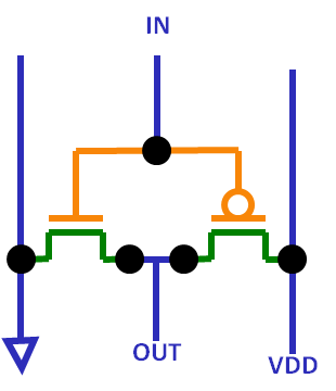
Schematic and layout are representing an inverter.
An inverter uses a NMOSFET and a PMOSFET.
The schematic shows the components and connections.
The layout has added different colors for different layers of the manufacturing process and each component.
These colors are transferred into the schematic showing the relationship between layout and schematic.
Wiring and transistor gates and diffusion have a minimum physical size of width and length of F.
There are also minimum distances required to prevent shorts.
It is difficult to automatically transform one view into the other.
A schematic is drawn to be able to easily understand the circuit. On the left is GND, on the right VDD, on the top inputs, on the bottom outputs.
In a schematic connection between 2 pins can be accomplished by labeling the pins with the same names. Lines can cross without resulting in short circuits.
A layout is drawn for symmetric and regular patterns, avoiding signal cross coupling and shape distortion, and having minimum size.
Operation of the MOSFET switch
| NMOS Logic 1 turns the switch on VGS = VDD connects Drain and source Logic 0 turns the switch off VGS = GND disconnects Drain and Source |
PMOS Logic 0 turns the switch on VGS = GND connects Drain and source Logic 1 turns the switch off VGS = VDD disconnects Drain and Source |
 |  |
| Inverter | Transmission gate |
MOSFET switch model
|
|
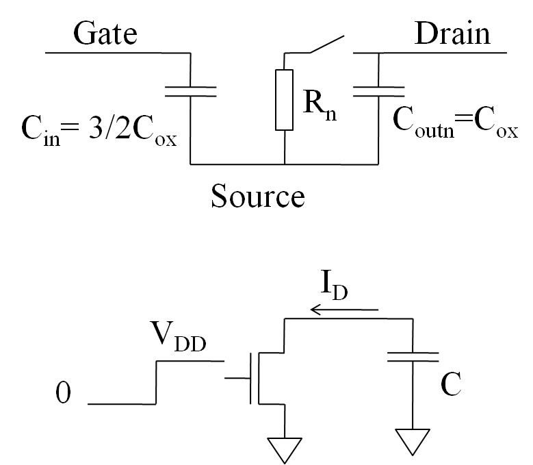
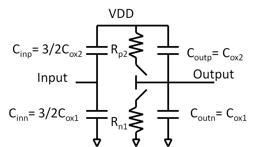
The equivalent input capacitance for a CMOS inverter can be calculated.
The input goes from low (GND) to high (VDD).
The output goes from high (VDD) to low (GND).
1/2 Cox is between Gate and source and 1/2 Cox is between gate and drain.
The gate drain capacitance sees twice the voltage swing giving an equivalent capacitance of Cox. Therefore the total input capacitance is:
\( C_{in} = \frac{3}{2} C_{ox} \)
The total output capacitance is:
\( C_{out} = C_{ox} \)
An amplifier with a high voltage gain of AV has an input capacitance of:
\( C_{in} = (A_{V} + 2) \frac{1}{2} C_{ox} \)
This is called the Miller effect.
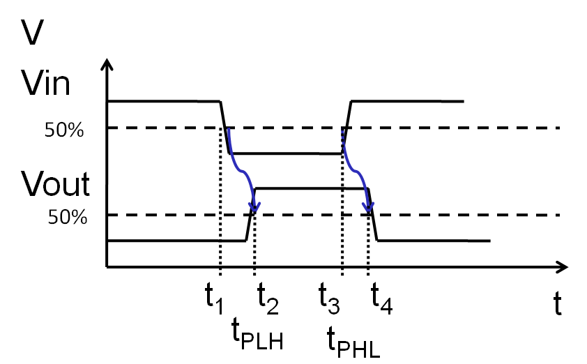
The propagation delay tp can be different for rising (LH) or falling (HL) edge at the output due to the on resistance of the PFET or NFET.
To take into account input capacitance and output resistance for a delay measurement a real source is needed before the device under test (DUT) and a real load is needed after the DUT.
Be careful when simulations are done with ideal sources and no load.
The input goes from low (GND) to high (VDD).
The output goes from high (VDD) to low (GND).
1/2 Cox is between Gate and source and 1/2 Cox is between gate and drain.
The gate drain capacitance sees twice the voltage swing giving an equivalent capacitance of Cox. Therefore the total input capacitance is:
\( C_{in} = \frac{3}{2} C_{ox} \)
The total output capacitance is:
\( C_{out} = C_{ox} \)
An amplifier with a high voltage gain of AV has an input capacitance of:
\( C_{in} = (A_{V} + 2) \frac{1}{2} C_{ox} \)
This is called the Miller effect.
The propagation delay tp can be different for rising (LH) or falling (HL) edge at the output due to the on resistance of the PFET or NFET.
To take into account input capacitance and output resistance for a delay measurement a real source is needed before the device under test (DUT) and a real load is needed after the DUT.
Be careful when simulations are done with ideal sources and no load.
Propagation delay
|
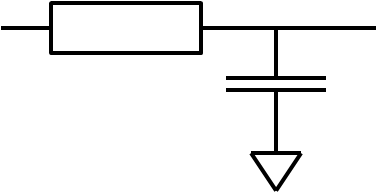
Charging of a capacitor (RC Delay) |
 |
|
Propagation Delay tP: Blue arrow Different between rising and falling edge. Different active transistors. |
|
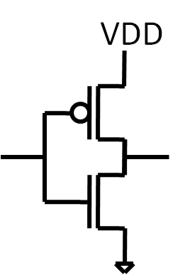
Inverter
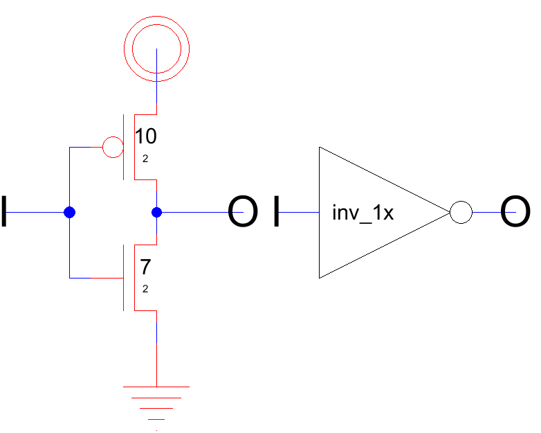
A schematic and logic symbol of an inverter is displayed.
The PFET at the top and NFET at the bottom can be seen.
The length and width are annotated at the transistors.
Since drawings are done with a precision of λ = 1/2 F width and length is given in λ.
The inverter can also give the sizing of PFET and NFET. Here an inverter with 1x size is given.
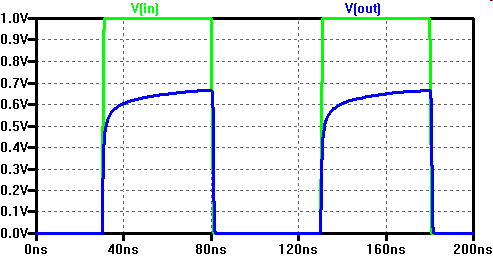
Transfer curve of an inverter
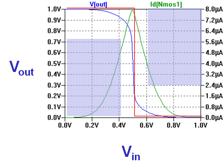
The red curve is the ideal transfer characteristic.
The blue curve is a real transfer curve.
Around the center (Vin = 0.5V) a small change in Vin will cause a big change in Vout. Gain is defined as:
\( v_v = \frac{d V_{out}}{d V_{in}} \)
The blue curve is a real transfer curve.
Around the center (Vin = 0.5V) a small change in Vin will cause a big change in Vout. Gain is defined as:
\( v_v = \frac{d V_{out}}{d V_{in}} \)
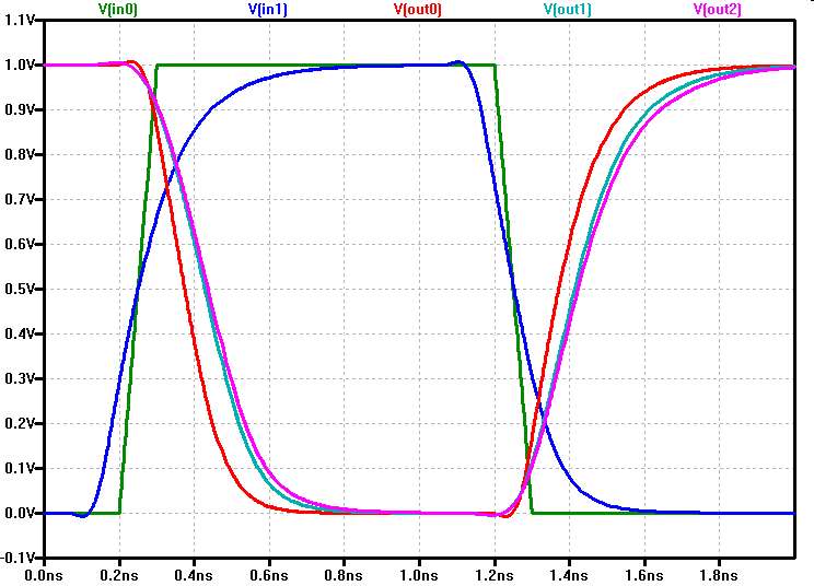
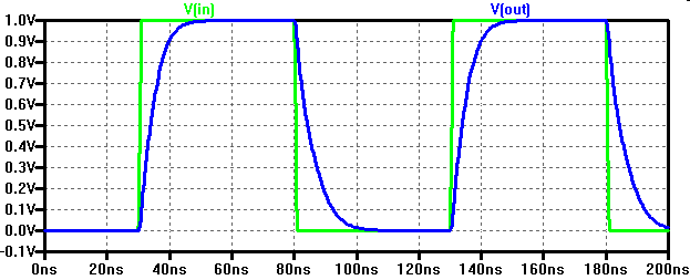
Switching of an inverter
Propagation Delay
The propagation delay of an inverter depends on source and load.
|
Always use a realistic source and load for delay investigations
Get typical delay times from the graph.
VIn0 In0 0 PULSE(0 1 0.2n 0.1n 0.1n 0.9n 2n)
VIn0b In0b 0 PULSE(1 0 71p 0.1n 0.1n 0.9n 2n)
In0b is the inverted signal of In0. It starts 129ps earlier than In0 to compensate for the delay of the first inverter.
In1 and In0 are aligned at 0.5V.
The delay depends not only on the investigated inverter, but on the slope of the input waveform and the load.
A high level delay model would take the drive strength of the input signal (slew rate, number of transistors, metal line length), the load capacitance and the drive strength of activated output transistors into account.
Furthermore it would take supply voltage and temperature into account.
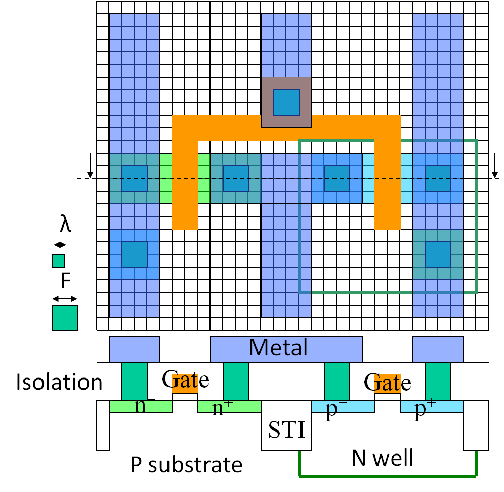
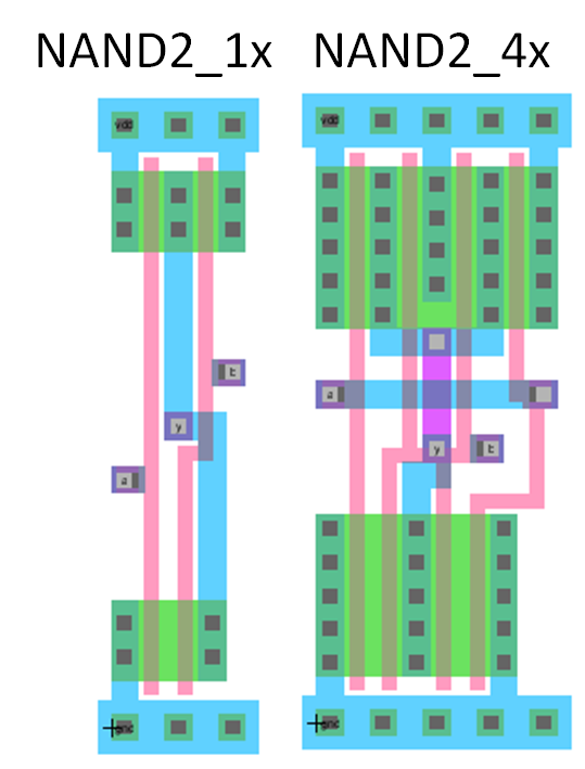
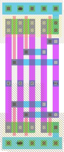
Standard cell: NAND layout
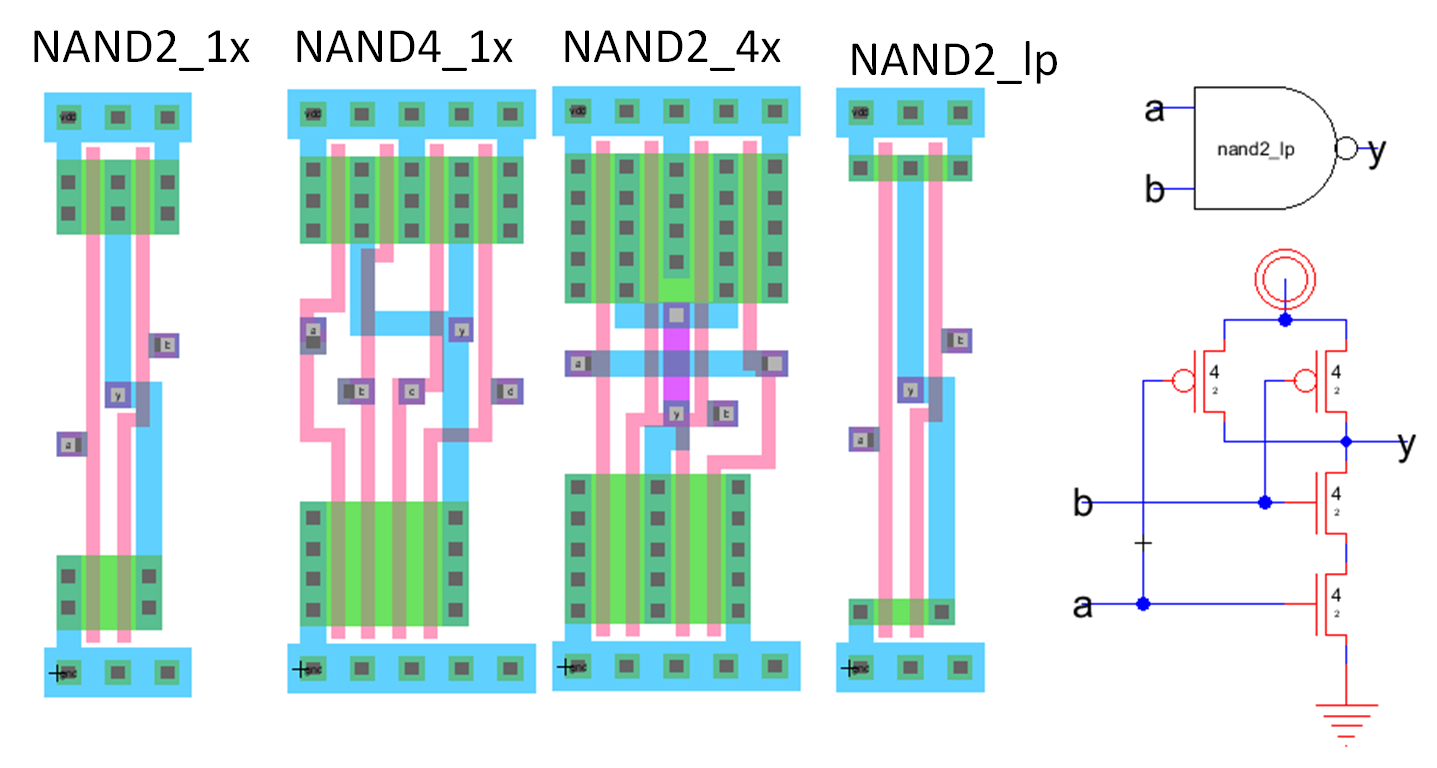
Transistors
Width determined by number of input and outputs
Same height, Names, vertical horizontal lines, exports, Hierarchy
Standard cell: Details
|
 muddlib07.jelib cells Not optimum for sub 100nm cells |
Standard cell sub 50 nm Feature Size
|
|
|
Pass gate and transmission gate
|
|
Switching of a pass gate
 |
\( t_{pPG} = 0.7 \cdot R_{DSon} \cdot ( C_{L} + \frac{C_{ox}}{2} ) \)
Switching of a transmission gate
 |
\( t_{pTG} = 0.7 \cdot (R_{DSonn} || R_{DSonp} ) \cdot ( C_{L} + \frac{C_{oxn}}{2} + \frac{C_{oxp}}{2} ) \)