Wafers and lots
|
  1 Lot: 25 Wafers |
Wafer are specified by diameter. A 200mm wafer has a radius of 100mm.
300mm, 8" ≈ 200mm, 6", 4", 3".
https://en.wikipedia.org/wiki/Wafer_(electronics)
300mm, 8" ≈ 200mm, 6", 4", 3".
https://en.wikipedia.org/wiki/Wafer_(electronics)
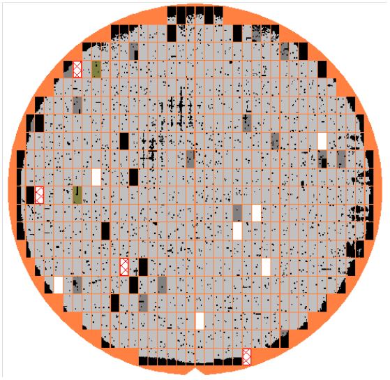
Wafer map 64 MBit memory chip (1997)
|
Number of Chips per Wafer: 38*20 – 2 *(1+1+2+4+5+7+10+16) - 2 *(1+2+3+5+7+9+13) = 760 – 172 = 588 Die Area Estimation 200mm wafer diameter: π * r *r /(number of chips) 31416 mm2 / 588 = 53.4 mm2 Technology 0.24 μm 8F2 Cell, 64 MBit Array Size : 64 MBit * 8 * 0.24 * 0.24E-6 mm2 = 30.1 mm2 |
Cell Efficiency :
Memory cell area / Die size =
30.1/53.4 = 56.4 %
Year: 1996
Absolute yield:
\( Y = \frac{N_{Good}}{N_{Total}} \)
Perfect yield: White chips
\( Y_{perfect} = \frac{7}{576} = 1.18 \% \)
Memory cell area / Die size =
30.1/53.4 = 56.4 %
Year: 1996
Yields:
Absolute yield:
\( Y = \frac{N_{Good}}{N_{Total}} \)
Perfect yield: White chips
\( Y_{perfect} = \frac{7}{576} = 1.18 \% \)
Example: Defect density and chip size
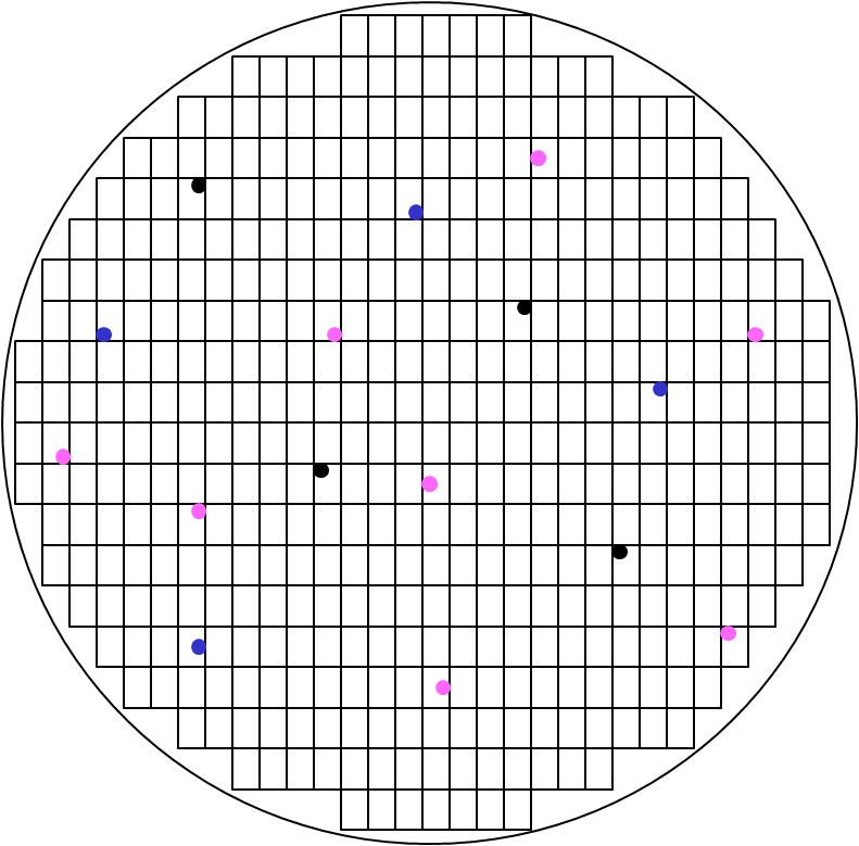
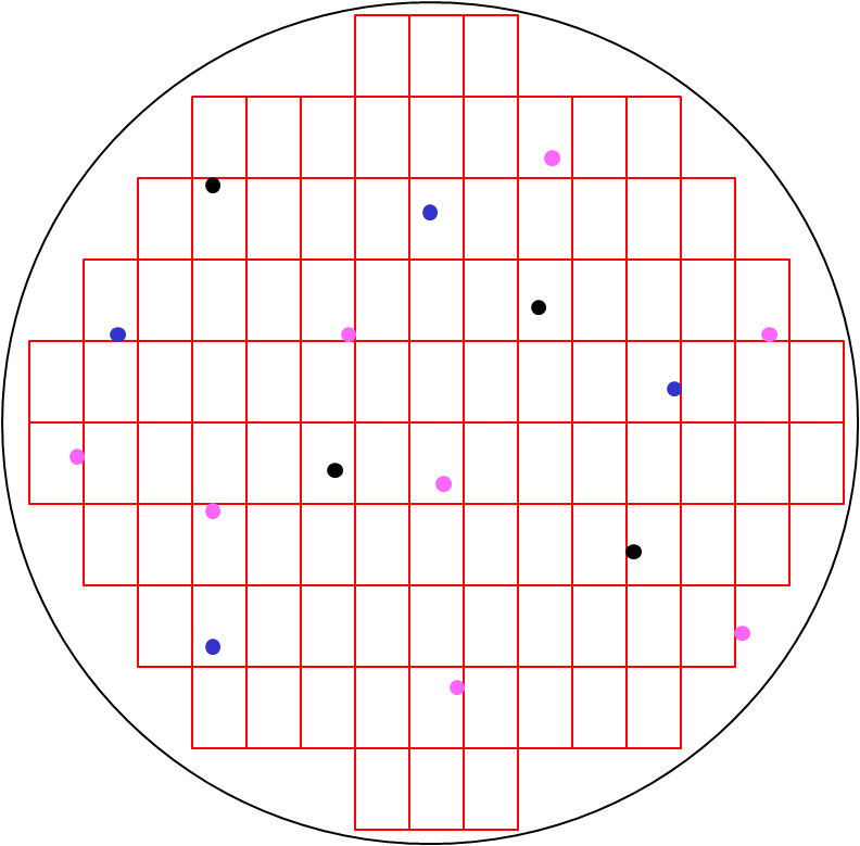
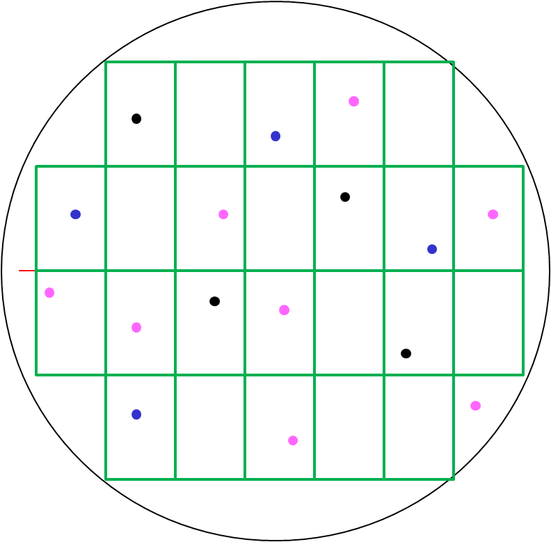 4 black defects, 4 blue defects, 8 pink defects
Size A, 4 A, 16 A
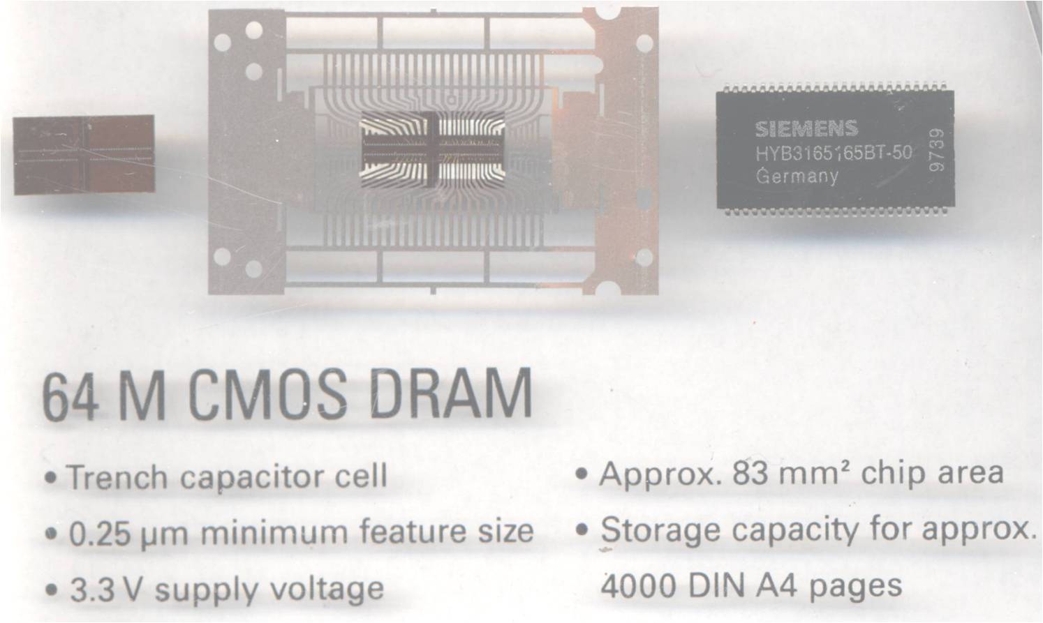
A memory chip 1997
Cross-section of microprocessor chip
Courtesy of International Business Machines Corporation. Unauthorized use not permitted.
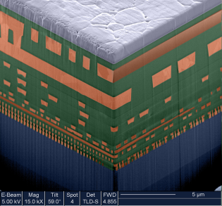
Cross-section of 64-bit high-performance microprocessor chip
Date added: 05 Dec 2005
Cross-section of 64-bit high-performance microprocessor chip built in IBM's 90 nm Server-Class CMOS technology with Cu/low-k wiring.
Above the transistors, the wiring levels include one W local interconnect, five "1x-scaled" Cu levels in full SiCOH low-k dielectric, three "2x-scaled" Cu/SiCOH levels, two "6x-scaled" Cu levels in FTEOS/SiO2 dielectric, and finally, one Al(Cu) terminal pad and wiring level.
The minimum M1 Cu line widths and spaces are 0.12 um.
Process steps
Pattern transfer with photo maskThe wafer is coated with photo resist. The pattern of a mask is transfered via light into the photo resist. The illuminated photo resist changes properties and is selectively removed. Photolithography DepositionOxide, nitride or metal can be deposited uniformly onto the wafer. EtchThere is chemical or plasma etch possible to remove material selectively. ImplantDopant ions (phosphor, boron) are electrically accelerated and shot into the wafer. After annealing at high temperature the dopants are activated. |

|