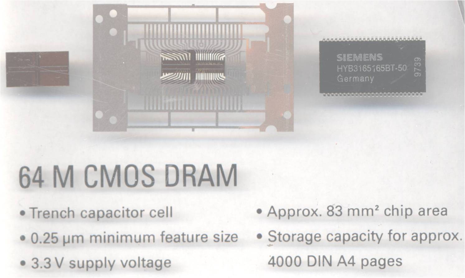
A 64MBit DRAM 1997
Author: Joerg Vollrath
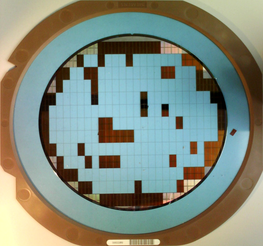
Wafer Carcass
Author: Joerg Vollrath
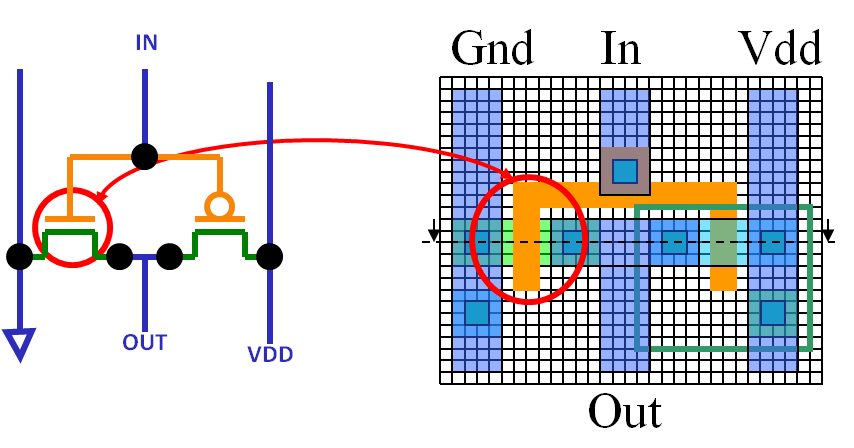
Matching Schematic versus Layout; Stick diagram
|
Symbols: Transistor, gnd, Vdd Properties: Names, width, length |
Layers, different color: Connection: metal (blue), polysilicon (orange,pink), contact (black) Transistor: crossing polysilicon and n- or p-diffusion (green) |
Before layouts are done stick diagrams can help planning.
This is shown on the right.
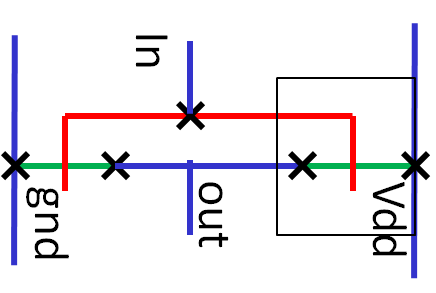
Only colored lines are used representing the layout.
Black crosses represent contacts.
Blue lines are metal, orange/red/pink lines are polysilicon, green lines are diffusion.
This is shown on the right.
Only colored lines are used representing the layout.
Black crosses represent contacts.
Blue lines are metal, orange/red/pink lines are polysilicon, green lines are diffusion.
MOSIS design rules
|
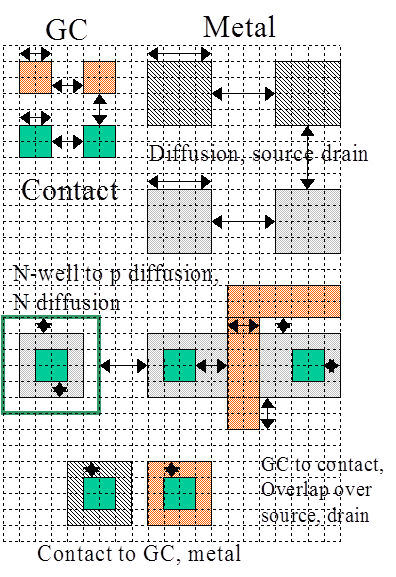 |
From Circuit to Chip
|
 |
Inverter Mask Set
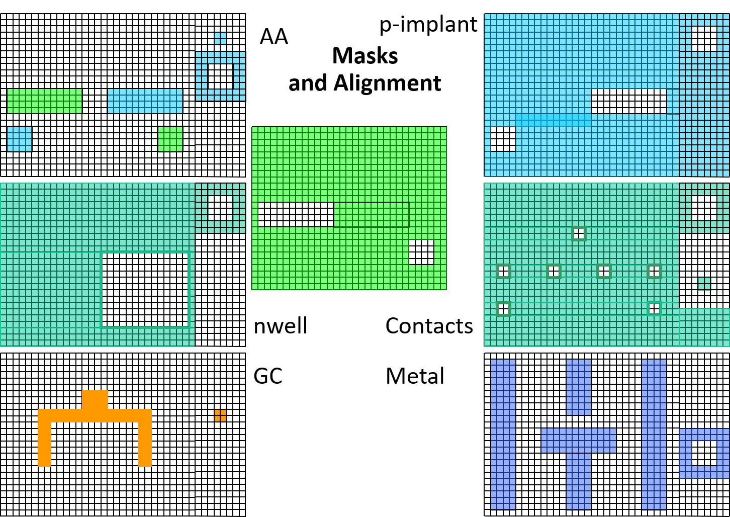
Author: Joerg Vollrath
Inverter Alignment
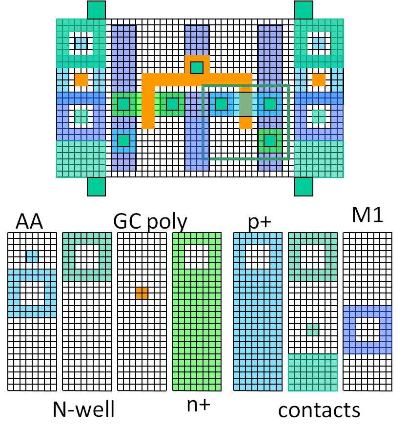
Author: Joerg Vollrath
Pattern Transfer
Patterns are transfered by illuminating a photoresist and changing the material
structure. During photo resist development the illuminated part is
chemically removed.
Patterns can change during this process.
Wavelengths to transfer patterns changed with feature size.
i-Line 365nm was used for 1.0..1.5µm.
248 nm from 1µm..180nm.
193 nm Deep ultra violett (DUV) from 180 nm..13 nm.
In the future for less than 10nm extreme ultra violett (EUV) could be used.
Since wavelength is bigger than the feature size immersion lithography and multiple patterning is used.
A liquid changes the wavelength of light.
With multiple patterning only an overlap of 2 structures is printed.
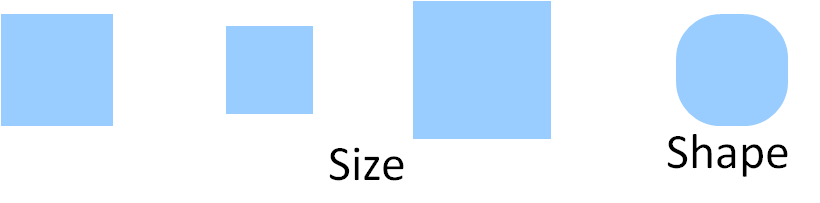
The shape of a feature is changed during the transfer.
- Size can change
- Edges and corners are rounded
- The shape can depend on the surroundings.
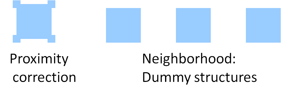
These errors can be precompensated by sizing, adding smaller features or dummy structures.
Also for chemical and mechanical processing a constant pattern density is needed for uniformity.
Dummy structures are used for that: GC fill, dummy contacts.
A common centroid layout should be used.
Patterns can change during this process.
Wavelengths to transfer patterns changed with feature size.
i-Line 365nm was used for 1.0..1.5µm.
248 nm from 1µm..180nm.
193 nm Deep ultra violett (DUV) from 180 nm..13 nm.
In the future for less than 10nm extreme ultra violett (EUV) could be used.
Since wavelength is bigger than the feature size immersion lithography and multiple patterning is used.
A liquid changes the wavelength of light.
With multiple patterning only an overlap of 2 structures is printed.
The shape of a feature is changed during the transfer.
- Size can change
- Edges and corners are rounded
- The shape can depend on the surroundings.
These errors can be precompensated by sizing, adding smaller features or dummy structures.
Also for chemical and mechanical processing a constant pattern density is needed for uniformity.
Dummy structures are used for that: GC fill, dummy contacts.
A common centroid layout should be used.
Overetch
Overetch, smaller lines causing opens
Author: Joerg Vollrath
Underexposure
Underexposure, fat lines causing shorts
Author: Joerg Vollrath
Translational misalignment causing shorts
Author: Joerg Vollrath
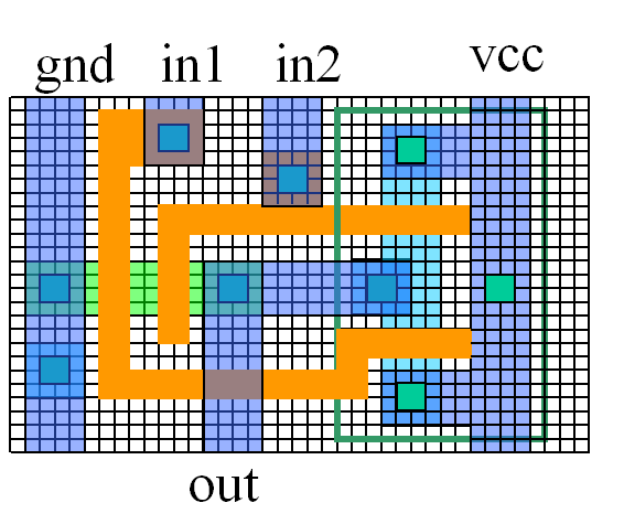
Problem Design Rule Check
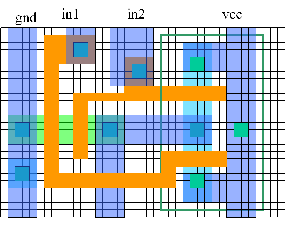
Author: Joerg Vollrath
Problem Design Rule Check
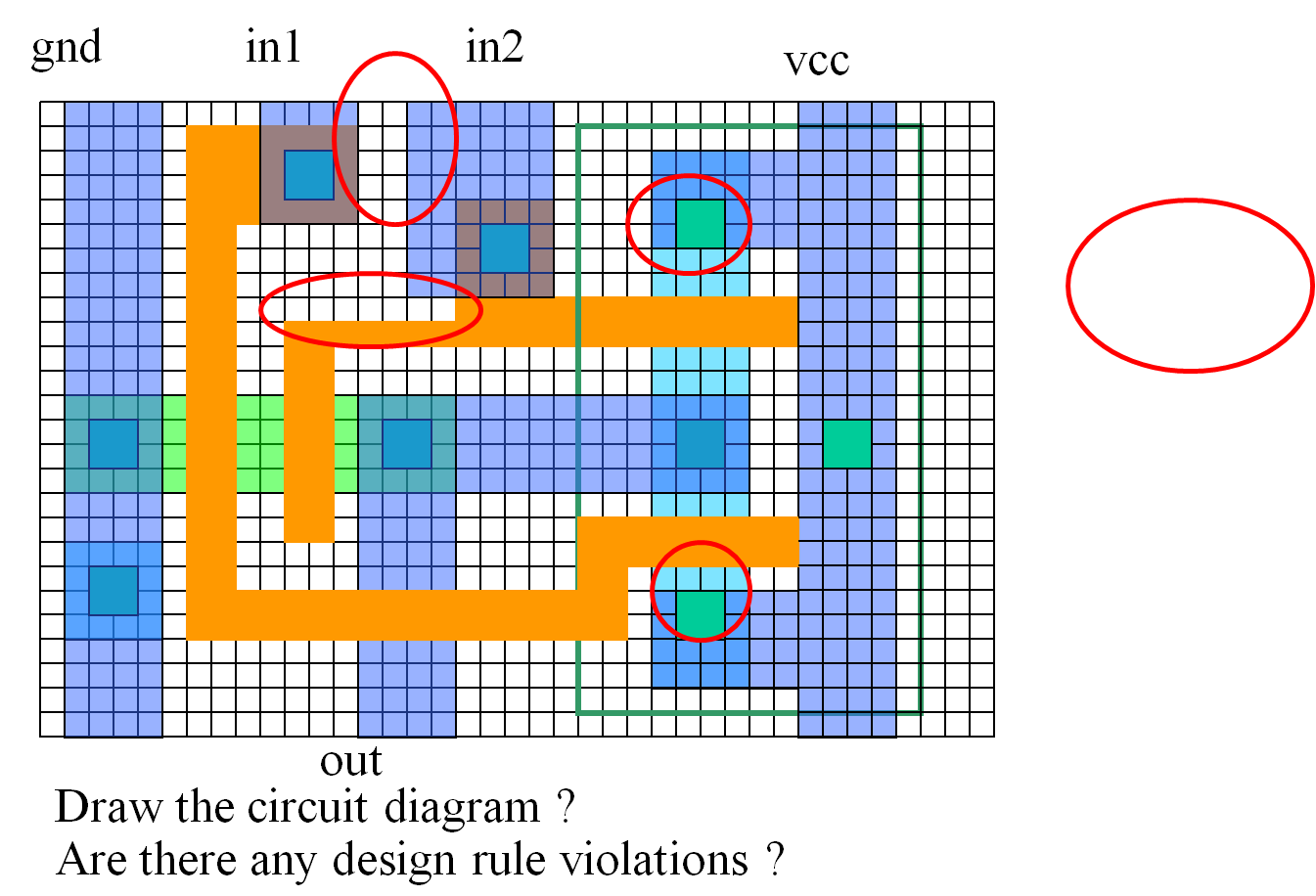
Author: Joerg Vollrath
Problem Design Rule Check
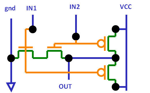
| In2 | In1 | Out |
| 0 | 0 | 1 |
| 0 | 1 | 1 |
| 1 | 0 | 1 |
| 1 | 1 | 0 |
Using the simple MOSFET switch model a NFET switch is closed,
if the input is 1. A PFET switch is closed, if the input is 0.
The path to ground 0V is only connected if In2 and In1 are 1. Then the output is '0'.
The path to ground 0V is only connected if In2 and In1 are 1. Then the output is '0'.