Devices Outline
|
|
MOSFETs are the building blocks of circuits.
There are also resistors and capacitances, which can be realized with transistors.
Sometimes circuit peformance is limited by parasitics.
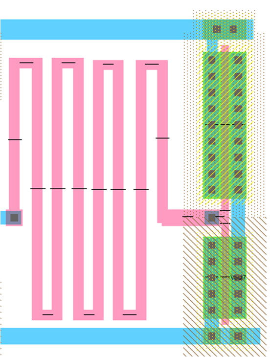
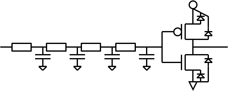
The layout above shows an input with along polysilicon line leading to an inverter.
There will be extra propagation delay because of the R and C of the polysilicon.
For real simulations of circuits parasitic R and C are extracted from layout and used.
An equivalent schematic with R and C and some parasitics diodes are shown below.
This lecture deals with resistors and capacitances in semiconductor technology.
There are also resistors and capacitances, which can be realized with transistors.
Sometimes circuit peformance is limited by parasitics.
The layout above shows an input with along polysilicon line leading to an inverter.
There will be extra propagation delay because of the R and C of the polysilicon.
For real simulations of circuits parasitic R and C are extracted from layout and used.
An equivalent schematic with R and C and some parasitics diodes are shown below.
This lecture deals with resistors and capacitances in semiconductor technology.
Resistance
|
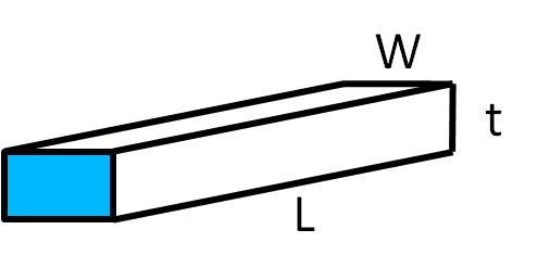
\[ R = \frac{\rho}{t} \frac{L}{W} = R_{square} \frac{L}{W} \]
R: resistance ρ : resistivity t: thickness L: length W: width Rsquare: sheet resistance |
\[ \rho = f(\mu_n, \mu_p, n(N_A), p(N_D), T) \]
μn, μp: mobility of electrons and holes ND, NA: doping concentration T: temperature non linear relationship |
 |
 |
Resistance of doped silicon
Temperature dependence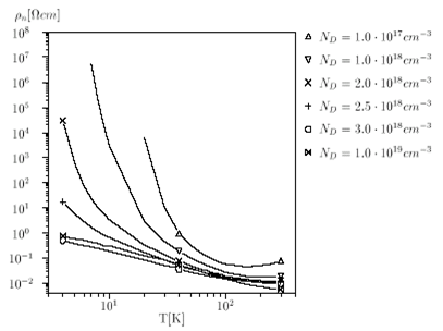
|
Doping dependence |
Thickness 180µm,
Sheet Resistance calculator, PV Lighthouse
| Doping concentration | 1E15 | 3E15 | 1E16 | 3E16 | 1E17 | 3E17 | 1E18 | 3E18 | 1E19 | 3E19 | 1E20 |
| n-sheet resistance | 360E3 | 102E3 | 30.5E3 | 11.2E3 | 4.21E3 | 1.94E3 | 920 | 485 | 233 | 109 | 42.6 |
| p-sheet resistance | 1069E3 | 299E3 | 86.5E3 | 30.1E3 | 10.3E3 | 4.28E3 | 1.82E3 | 888 | 398 | 178 | 66.4 |
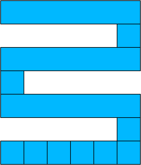
Layout of resistors
|
Avoiding long lines Serpentine Avoid corners with extra contacts Count number of squares along resistor and multiply with sheet resistance: 27 squares N-poly silicide: 5Ω/square R = 27 * 5 Ω = 135 Ω |
|
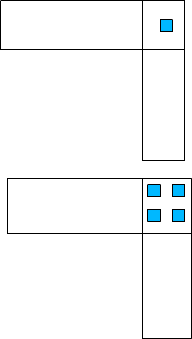
Contact Resistance
|
10Ω/contact Unit contacts More contacts are better Parallel connection \[ R_{total} = \frac{R}{n} \] |
|
Maximum current density and electromigration
|
Metal: Electromigration 1..2mA/µm Electromigration is the transport of material caused by the gradual movement of the ions in a conductor due to the momentum transfer between conducting electrons and diffusing metal atoms. The effect is important in applications where high direct current densities are used, such as in microelectronics and related structures. As the structure size in electronics such as integrated (ICs) decreases, the practical significance of this effect increases. |


|
Supply voltage routing
|
0.1 Ω/square AreaChip = 100 mm2 Line length up to 10 mm. 200 nm width of line. 50 000 squares R = 5 kΩ Current: 40 µA; Voltage drop: Vdrop = I * R = 0.2 V VDD = 1 V Vinverter = 1 V - 2 * 0.2 V = 0.6 V Vthn = 0.3 V; Vthp = -0.3 V; |
 |
Capacitances
Reference: CMOS, Circuit Design, Layout and simulation, Baker, Chap. 4, p.61 |
|
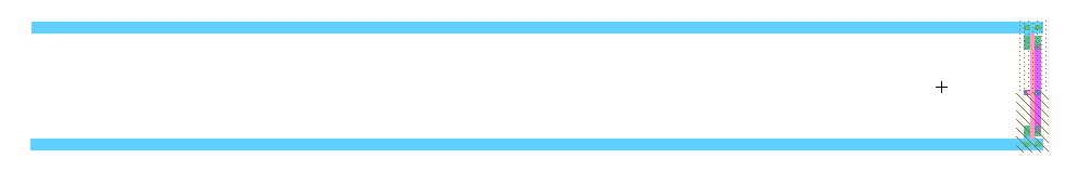
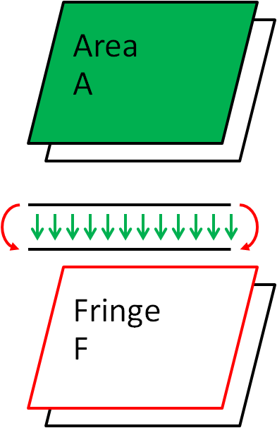
- Area capacitance: plate capacitance
\( C = \epsilon_0 \cdot \epsilon_{SiO2} \frac{A}{d} \)
ε dielectric constant
A: plate area
d: distance between electrodes, thickness of isolator - Fringe capacitance
Example poly silicide resistor
|

|
Example Inverter
|
|
Design Tool RCX
- Resistor and capacitance extraction from layout
- Electric: Preferences, Tools, Technology, SPICE
- More realistic delays
- More realistic power distribution
- More simulation time
Example
|
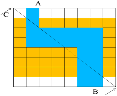
A top view of a metal line in a 50nm process running from A to B is
shown crossing a polysilicon line, which runs from left to right. The
metal sheet resistance is Rsquare=0.6Ω/square. The lines are isolated with 80nm oxide. (ε0= 88 fF/cm, εSiO2 = 4) 1. Calculate the capacitance between the metal line (blue) and the polysilicon line (yellow).(2 points) 2. Calculate the resistance from A to B? (2 points) 3. Calculate the voltage drop on the line if a current of 30µA is flowing. (2 points) 4. Draw a cross section from points C to D (4 points) |
 |
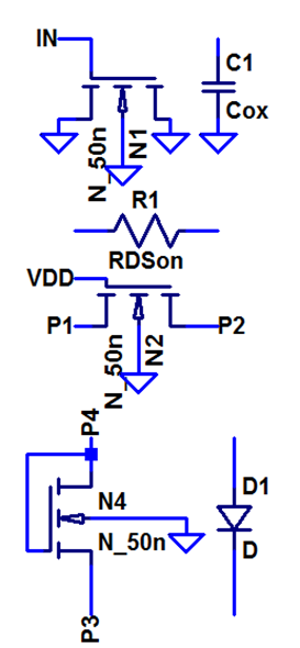
MOSFET used for other purposes
|
Capacitance Resistance Diode |
|
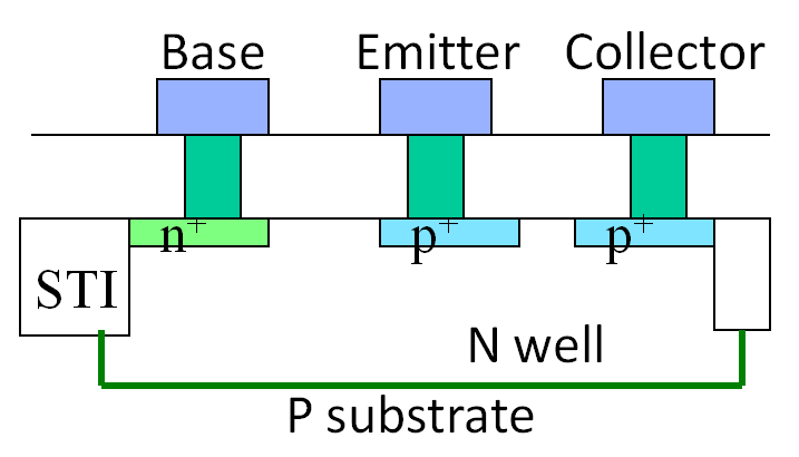
| Lateral bipolar transistor |
|
MOSFET and FINFET
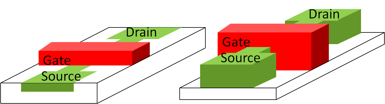
MOSFET |
FINFETFeature size sub 25 nm Fixed transistor width Channel surrounded by gate |
Nanosheet Transistor (2021)
NanosheetNFET and PFET on top of each other |
FINFETFixed transistor width Channel surrounded by gate |
Feature size < 5nm
Name: gate-all-around, multibridge channel, nanobeam, nanosheet
The Nanosheet Transistor Is the Next (and Maybe Last) Step in Moore’s Law?
Name: gate-all-around, multibridge channel, nanobeam, nanosheet
The Nanosheet Transistor Is the Next (and Maybe Last) Step in Moore’s Law?
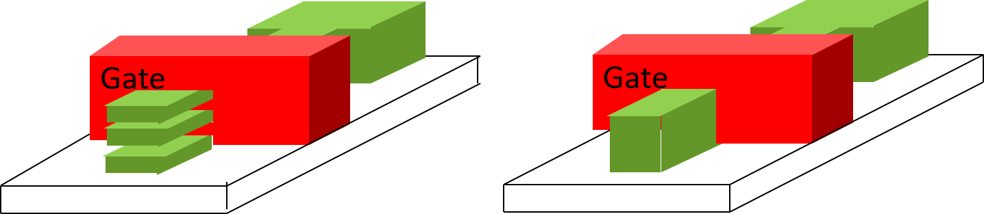
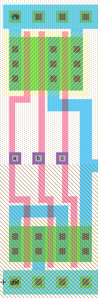
Stick diagram 3-input NAND (10.05.2023)
Use lines to draw a circuit
 |
 |
Stick diagrams are used for layout planning.
It is very easy to draw lines and squeeze lines between 2 other lines.
This action would be much harder with rectangles with minimum feature size and distance.
When the stick diagram is finished it is easy to make a step by step plan for drawing the layout.
It is very easy to draw lines and squeeze lines between 2 other lines.
This action would be much harder with rectangles with minimum feature size and distance.
When the stick diagram is finished it is easy to make a step by step plan for drawing the layout.
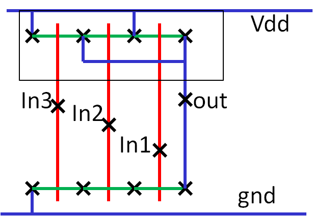
AOI design style
NAND\( Y = \overline{ X1 \cdot X2 \cdot X3} \) |
NOR\( Y = \overline{ X1 + X2 + X3} \) 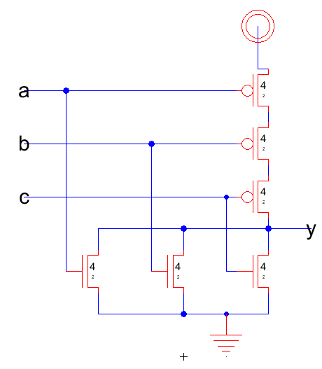 |
PFETs connected to VDD are at the top and NFET connected to GND at the bottom.
A NAND has PFETs on the top in parallel and NFETS at the bottom in series.
A NOR has PFETs on the top in series and NFETS at the bottom in parallel.
This can be used for arbitrary functions.
There can be additional inverters added to the inputs or outputs to realize a logic function.
Easy automated implementation with unit transistors is the main goal in this lecture. Power or speed optimization can be found in the literature and is extensively discussed. A lot of time can be spent to optimize the circuit.
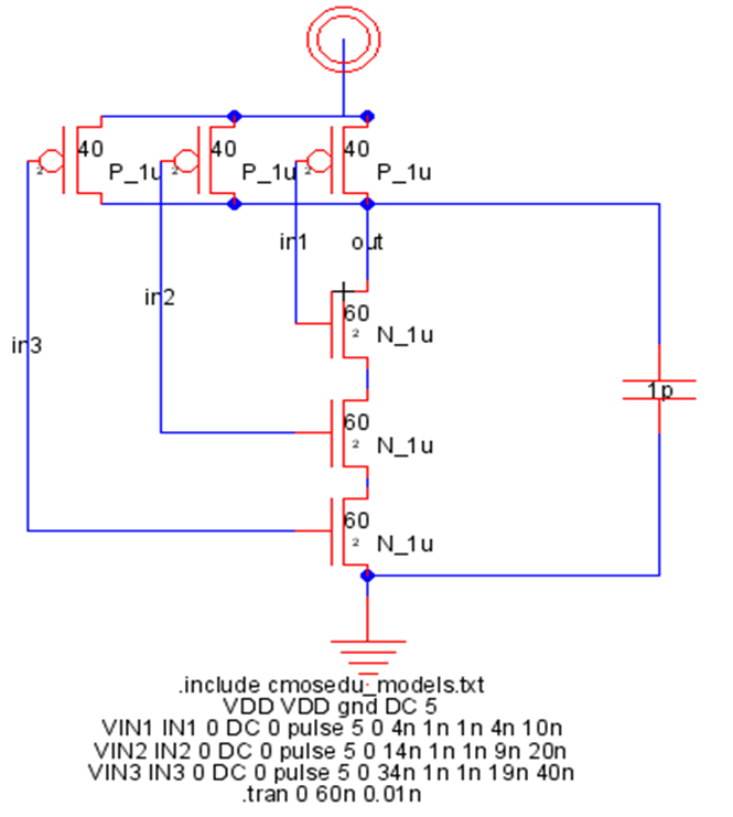
AOI design style example
|
\( Y = \overline{ (a + b) \cdot c} \) |
 |
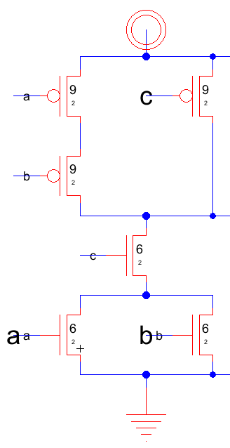
The (a + b) OR part of the function is realized as parallel NFETs at the bottom
and series PFETS at the top.
The AND function is realized as series NFETs at the bottom and parallel PFET at the top.
Baker, CMOS Circuit Design, 12.4
The AND function is realized as series NFETs at the bottom and parallel PFET at the top.
Baker, CMOS Circuit Design, 12.4
Implementation of bigger truth tables
|
Provide all 16 possible 2 input functions. |
Use a multiplexer for additional inputs. Example: LUT4_37E5 | ||||||||||||||||||||||||||||||||||||||||||||||||||||||||||||||||||||||||||||||||||||||||||||||||||||
|
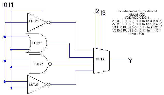 |
The picture shows implementation of a 4 input truth table.
Inputs are I0,I1,I2,I3.
The sequence of column sin the truth table has to be matched with the schematic.
The sequence of y shows first the LSB and then the MSB.
This is implemented in sclib.jelib
The SPICE code for simulation of the truth table is included here.
Inputs are I0,I1,I2,I3.
The sequence of column sin the truth table has to be matched with the schematic.
The sequence of y shows first the LSB and then the MSB.
| Nr | I3 | I2 | I1 | I0 | Y | Hex |
| 0 | 0 | 0 | 0 | 0 | 1 | 5 |
| 1 | 0 | 0 | 0 | 1 | 0 | |
| 2 | 0 | 0 | 1 | 0 | 1 | |
| 3 | 0 | 0 | 1 | 1 | 0 | |
| 4 | 0 | 1 | 0 | 0 | 0 | E |
| 5 | 0 | 1 | 0 | 1 | 1 | |
| 6 | 0 | 1 | 1 | 0 | 1 | |
| 7 | 0 | 1 | 1 | 1 | 1 | |
| 8 | 1 | 0 | 0 | 0 | 1 | 7 |
| 9 | 1 | 0 | 0 | 1 | 1 | |
| 10 | 1 | 0 | 1 | 0 | 1 | |
| 11 | 1 | 0 | 1 | 1 | 0 | |
| 12 | 1 | 1 | 0 | 0 | 1 | 3 |
| 13 | 1 | 1 | 0 | 1 | 1 | |
| 14 | 1 | 1 | 1 | 0 | 0 | |
| 15 | 1 | 1 | 1 | 1 | 0 |
This is implemented in sclib.jelib
The SPICE code for simulation of the truth table is included here.