Systems
FPGAField programmable gate array (FPGA)
|
 Switch matrix, logic and registers, programmable |
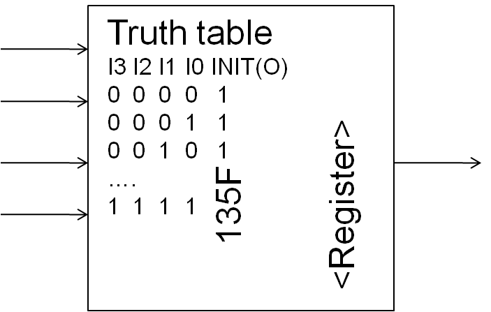
Xilinx FPGA configurable lookup table
Logic, register (folder: netgen/synthesis
|
 |
Books: FPGA Programming and VHDL
Rapid Prototyping of Digital Systems:Quartus® II Edition Hamblen 71.- Euro FPGA Prototyping by VHDL Examples:Xilinx Spartan-3 Version Chu 68.99.-Euro |

|
FPGA vendors: Intel(Altera), Xilinx
Xilinx WebPack free to download
Microelectronics Design Optimization
- Technology:
- FPGA, Gate Array, Standard cells, Full custom
- Design
- SystemC, VHDL/Verilog (RTL), Schematic
- Block technology:
- CPU, State machine
- Synchronous logic, asynchronous logic
- Memory: SRAM, RAM, NAND Flash
- CMOS logic style
- AOI, dynamic, transfer gate (TG), dynamic CMOS, domino
- Layout style
- Regular, full custom, transistor sizing
Goal: Time to market, timing and propagation delay, power, area
Gate Array, Semi-Custom, and Full-Custom ICs
|
Gate Array (biggest): Everything is prefabricated except metal connection Standard cells: Logic cells are placed and routed Full custom (smallest): Each gate is individually drawn and routed. Area ratio: 3:2:1 |

|
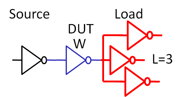
Timing Closure and Propagation Delay
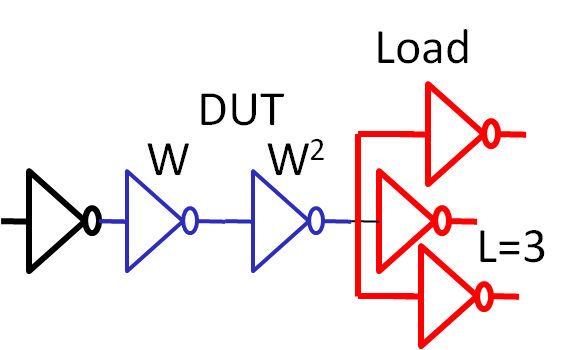
Measuring propagation delay requires a real driver to measure the influence of input capacitance and a real capacitance load to be charged. In the center is the DUT (device under test).
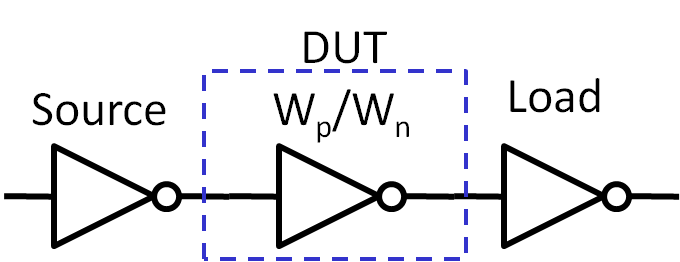
- Propagation Delay:
\( t_{delay} = 0.7 R C_{tot} \)
R: on resistance of PFET/NFET Ron; C: load capacitance - Changing Wp/Wn
Input capacitance changes, Ron changes
Smaller Ron and bigger input capacitance
How to optimize timing performance?
No premature optimization!
Start with minimum size, identify timing limit and then optimize.
Propagation Delay
- Propagation Delay
- Source inverter, DUT and load inverter minimum size: R, C
- tdelay = tdelayin + tdelayout = 0.7 R CDUTin + 0.7 RDUTon C
- R: on resistance of PFET/NFET
- C: load capacitance
- Changing all Wp/Wn
- Increasing width: Rnew= R/2, Cnew= 2 C
- tdelay = tdelayin + tdelayout = 0.7 R/2 2 CDUTin + 0.7 RDUTon/2 2 C
- No change in speed, higher power consumption, more area
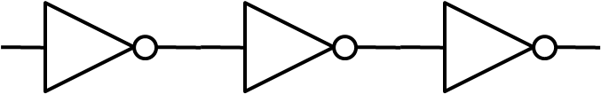
Topology and Propagation Delay
| Inverter chain |
|
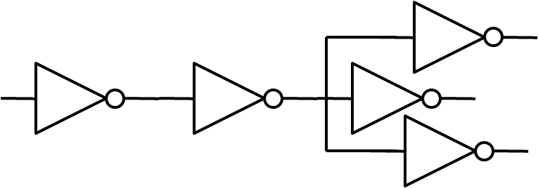
| Load: Driving a line or multiple logic gates |
|
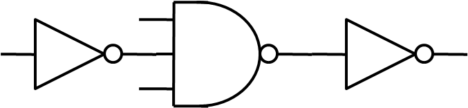
| Transistors in series or parallel |
|
Propagation Delay and Load
|
tdelay = tdelayin + tdelayout = 0.7 R · (W · C) + 0.7 (R/W) (L · C)
tdelay = 0.7 R · C ( W + L/W) = tdelay0 ( W + L/W)
Delay with large loads can be reduced with width W.
Using unit transistors W should be an integer number.
tdelay(L=1) = tdelay ( W + 1/W)
tdelay(L=5) = tdelay ( W + 5/W)
tdelay(L=10) = tdelay ( W + 10/W)
Current is needed to charge and discharge capacitances.
\( C = \frac{Q}{V} = \frac{I \cdot t}{V} \)
\( I = \frac{C \cdot V}{t} = C \cdot V_{DD} \cdot f_{CLK} \)
PAVG= VDD2 · C · fCLK
This is the active power consumption.
There are also cross currents from VDD to gnd during switching and transistor leakage currents.
Changing W to larger values increases power consumption.
tdelay(L=5) = tdelay ( W + 5/W)
tdelay(L=10) = tdelay ( W + 10/W)
Power
PAVG= VDD · IAVGCurrent is needed to charge and discharge capacitances.
\( C = \frac{Q}{V} = \frac{I \cdot t}{V} \)
\( I = \frac{C \cdot V}{t} = C \cdot V_{DD} \cdot f_{CLK} \)
PAVG= VDD2 · C · fCLK
This is the active power consumption.
There are also cross currents from VDD to gnd during switching and transistor leakage currents.
Changing W to larger values increases power consumption.
Propagation Delay and Load
|
tdelay = tdelayin + tmid + tdelayout = 0.7 R W CDUTin + 0.7 RDUTon/W W * W C + 0.7 RDUTon/W/W L C = tdelay ( W + W + L/W/W)
L: Load, W: Width
For higher loads use more than one stage.
Propagation Delay and Logic function
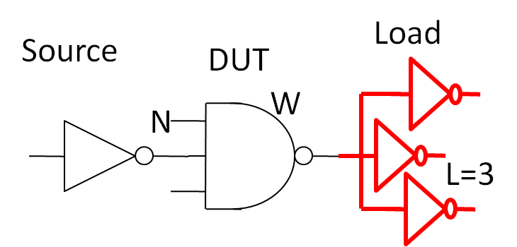
|
tdelay = tdelayin + tdelayout = 0.7 R W CDUTin + 0.7 N RDUTon / W * C * L = tdelay ( W + N / W * L)
Change only width W of series transistors
tdelay1 = tdelayin + tdelayout = 0.7 R (0.5 + 0.5 W ) CDUTin + 0.7 N RDUTon/ W C * L = tdelay ( 0.5 + 0.5 * W + N / W *L )
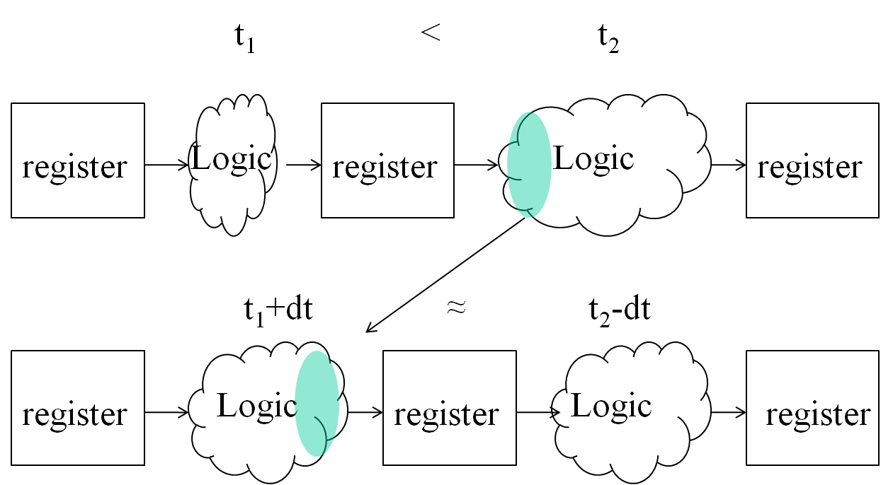
Propagation Delay and Pipelines
What is the maximum clock frequency?tpd = 5 ns, tsetup = 1 ns
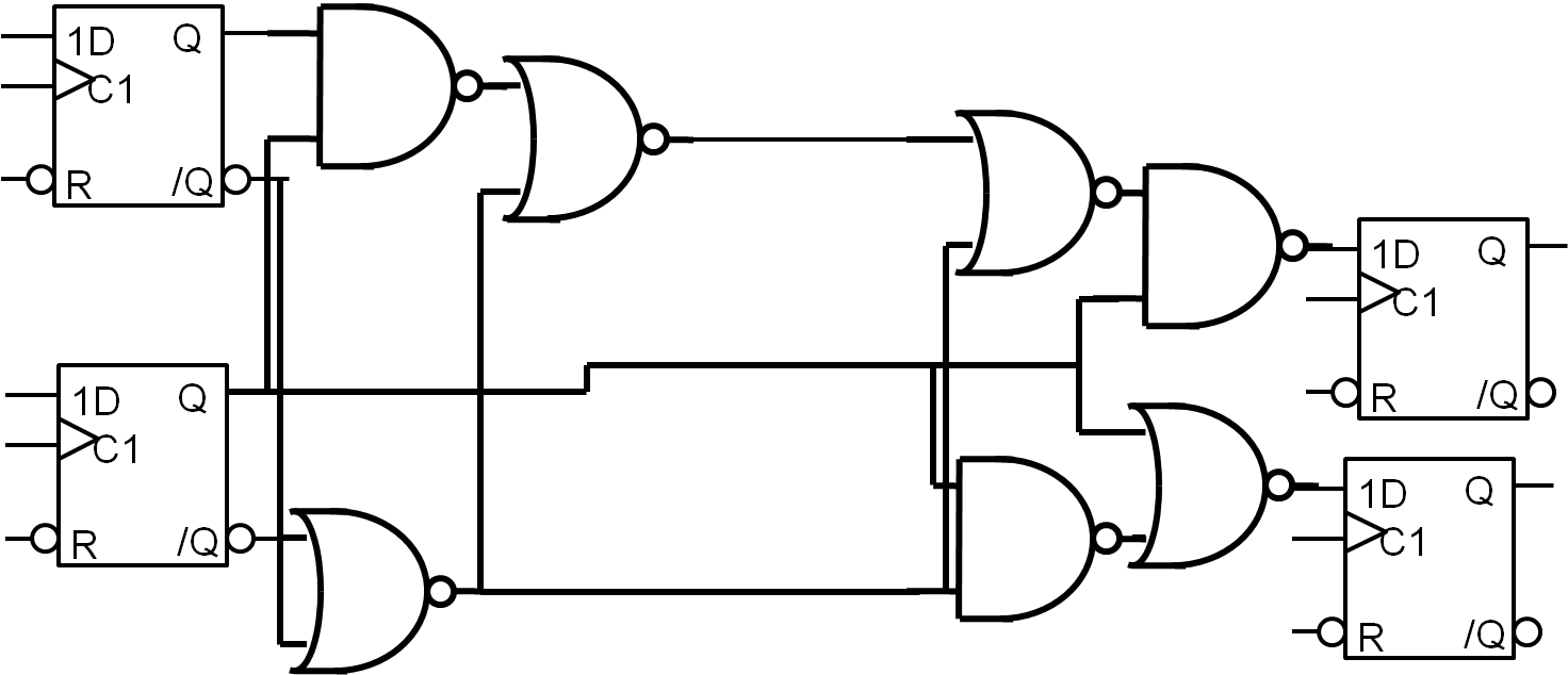
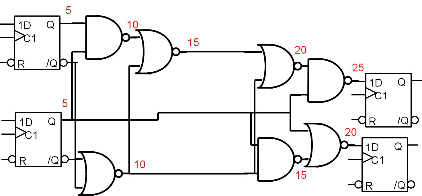
Retiming of synchronous logic