MIPS R3000A
|
32-bit 2nd generation commercial processor (1988) Led by John Hennessy (Stanford, MIPS Founder) external L1 Caches 1.2 µm process 115 K Transistor 20..33.3 MHz 48 mm2 die 145 I/O Pins VDD = 5 V 4 Watts SGI Workstations Wikipedia |

|
Intel processor
 |
Intel 4004 1971 2300 Tr. 4-Bit 500kHz 10 µm |
 |
Intel 8086 1978 29 kTr. 16-Bit 8 Mhz 3.2 µm 33 mm2 |

|
Intel 386 1985 275 kTr. 32-Bit 33 MHz 1.5 µm |

|
Intel Pentium 1993 3.1 MTr. 32-Bit 300 MHz 0.8µm 294mm2 |
Memory looks regular, logic has a random pattern in the chip top view pictures.
Over time more and more area was used for memory.
Due to miniaturization and minimum voltage limit (1V) the power density limits the maximum opeating speed.
Since there is a Vth distribution over the chip and wafer it is difficult to realize a Vth < 300mV. Therefore minimum Vdd = 1V.
Latest integrated circuits: more cores, just copy a block a couple of times and add glue logic
Microelectronics Limits
- Feature size: Wave length of light source, a few nm
- Feature size: Number of atoms needed for creating n, p regions with doping (100..1000), a few nm
- Supply voltage: dielectric break down and statistic Vth variation VDD = 1 V
- Power density: clock rate limit 3 GHz
D-Flip-Flop
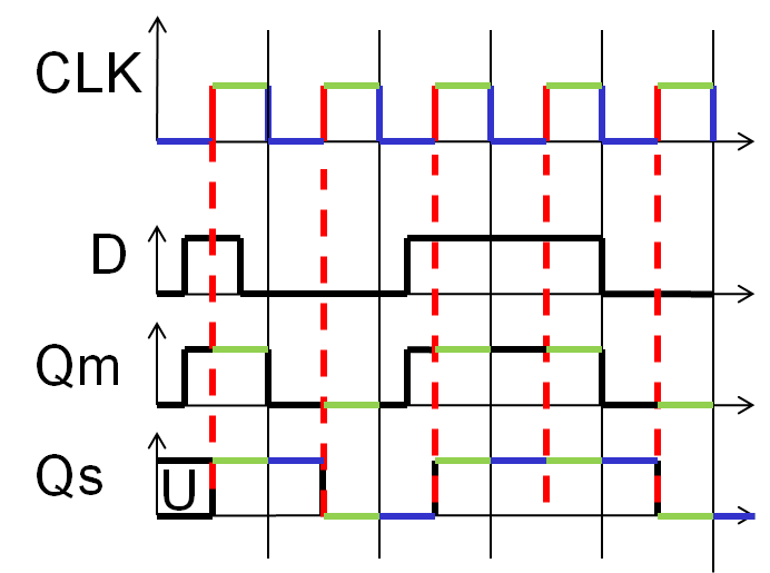 |
This circuit shows a positive edge triggered D-Flip-Flop (DFF).
Data of input D is latched at a rising clock edge (CLK) and Qs and Qb are holding this data until the next rising clock edge.
This is the only relevant flip flop used in digital circuits.
A reset input and testability inputs can be added as shown later.
Data of input D is latched at a rising clock edge (CLK) and Qs and Qb are holding this data until the next rising clock edge.
This is the only relevant flip flop used in digital circuits.
A reset input and testability inputs can be added as shown later.
Setup and Hold Time
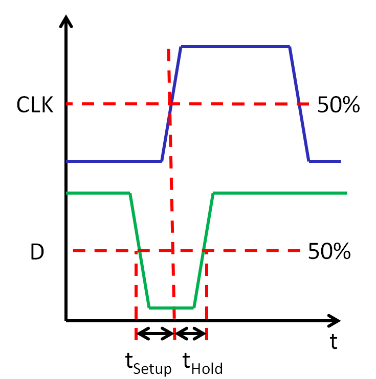
Important timing parameters are setup and hold time of a DFF.
Setup time is needed to transfer the input level to the internal inverters.
Setup time and propagation delay are limiting the maximum clock frequency.
Setup time is needed to transfer the input level to the internal inverters.
Setup time and propagation delay are limiting the maximum clock frequency.
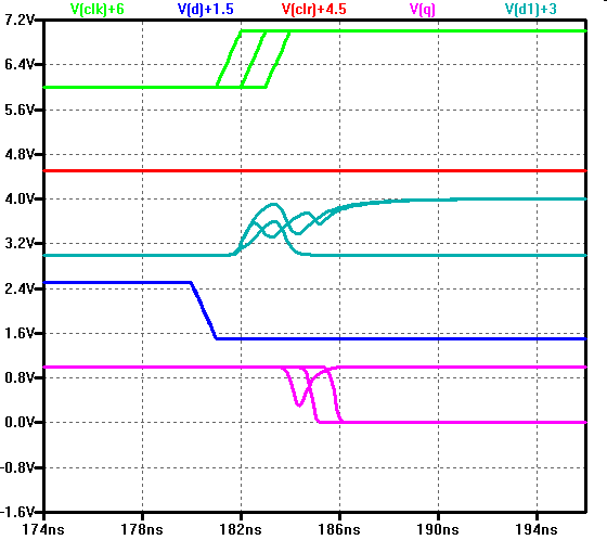
Setup and Hold Time, SPICE Simulation
|
Vary positive CLK edge in regard to input data Not enough setup time, bad output Minimum setup time Register delay from rising clock to output Shmoo plot
VDD
1.2V |xxxxx......|
1.1V |xxxxx......|
1.0V |xxxxx......|
0.9V |xxxxx......|
0.8V |xxxxx......|
-0.5n 0.5n
tsetup
X: Fail
|
 Simulation waveform DFF_test.asc |
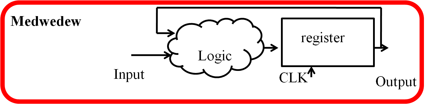
Medwedew Finite State Machine
Maximum clock frequency:tCLK > tpdLogic + tsetup + tpdRegister
There are also Mealy and Moore state machines, which make testing more complicated
State diagram, state transition table
 State Diagram
|
|
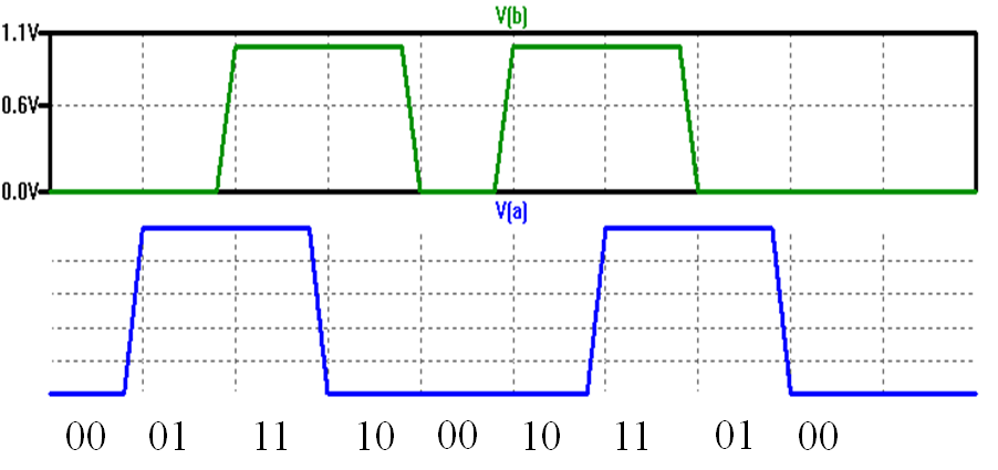
Truth table and test
|
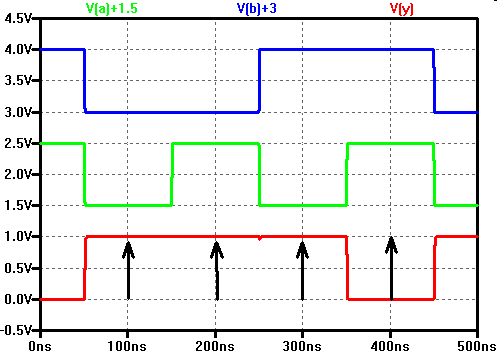 | ||||||||||||||||||
Each line in the truth table is one column, a certain time in simulation or measurement.
All possible combinations have to be tested to prove correct function.
Due to propagation delay output signals are shifted to the right.
Expected output signal is compared to real output signal at certain times (arrows).
All possible combinations have to be tested to prove correct function.
Due to propagation delay output signals are shifted to the right.
Expected output signal is compared to real output signal at certain times (arrows).
NAND Gate Simulation with Error
|
Observability of errors requires real voltage sources (Rser).
Missing wires, connections and high ohmic connections are simulated.
Bad behaviour can be seen. The analog output value has to be converted to '0' or '1' using mid level.
It can also be seen, that over time output level is sometimes changing.
This can be a delay fault or a memory effect.
If there is a switch and a capacitor available memories are created.
It is more difficult to test memories.
Pure Logic Test
|
|
|
||||||||||||||||||||||||||||||||||||||||
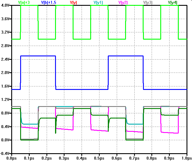
Scannable D-Flip-Flop
Additional pins:|
SE/TE:scan/test enable SDI/TDI: scan/test data in SDO/TDO: scan/test data out Shift register to set and read register 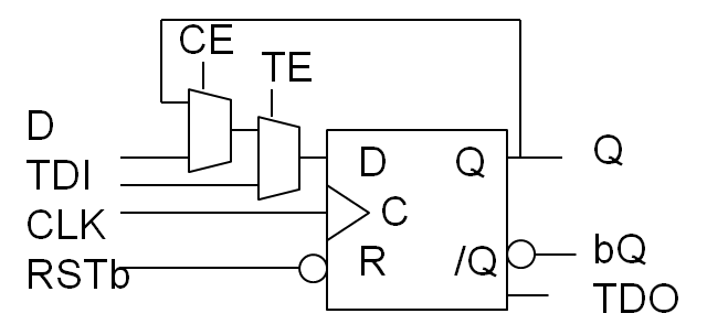
|
Scan Flip Flop: Simulation
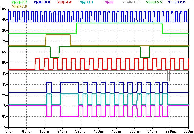
800ns simulation time with CLK cycle 20ns gives 40 test vectors.
LTSPICE simulation code:
Each row in the state table is a CLK cycle column in the simulation.
Simulation starts with CE low.
Betwenn 166 ns and 274 ns TE operation is checked.
At 300 ns CE goes active. D is transfered into the D-FF.
At 705 ns reset is applied and the output Q goes to 0.
Is the testing complete?
Is the circuit working correctly?
Test coverage:
25 = 32 input combinations (vectors).
TE,RSTb,CE,D,TDI: 010X1, 110XX, 011XX, 00001
11 combinations tested
TC = 11/32 = 34.3%
JavsScript generating test vectors: TestJS.html
Nr CE TE TDI D RSTb xTDO xQ xQB
 0  0  0   1 0 1    1    1  0   Start 6x
 6  0  0   1 1 1    1    1  0   Keep state
 7  0  0   1 0 1    1    1  0   Keep state
 8  0  1   1 1 1    1    1  0   TE active
LTSPICE simulation code:
.global VDD
.option TEMP 90
VDD VDD 0 DC 1
VCLK CLK 0 PULSE(0 1 0n 1n 1n 8n 20n)
VCE CE 0 PULSE(0 1 300n 1n 1n 380n 600n)
VCLR RSTb 0 PULSE(1 0 705n 1n 1n 8n 2800n)
VD D 0 PULSE(0 1 117.2n 1n 1n 18n 40.05n)
VTDI TDI 0 PULSE(1 0 185n 1n 1n 38n 400n)
VTE TE 0 PULSE(0 1 165n 1n 1n 108n 2800n)
.include cmosedu_models.txt
.tran 0 800n
Each row in the state table is a CLK cycle column in the simulation.
Simulation starts with CE low.
Betwenn 166 ns and 274 ns TE operation is checked.
At 300 ns CE goes active. D is transfered into the D-FF.
At 705 ns reset is applied and the output Q goes to 0.
Is the testing complete?
Is the circuit working correctly?
Test coverage:
25 = 32 input combinations (vectors).
TE,RSTb,CE,D,TDI: 010X1, 110XX, 011XX, 00001
11 combinations tested
TC = 11/32 = 34.3%
JavsScript generating test vectors: TestJS.html
Application: Tiny FPGA
|
How many test vectors are needed? How many subcircuits to test? How to document test vectors? |

|
This was a laboratory task.
This circuit demonstrates an FPGA with 2 inputs (I0, I1), lookup table LUT2, switches (MUX) and outputs O0, O1.
Internal output signals Y can be fed back with Y0, Y1 to the input MUXes for state machines.
The TE, TDI, TDO interface configures MUX and LUT2 circuits.
This circuit demonstrates an FPGA with 2 inputs (I0, I1), lookup table LUT2, switches (MUX) and outputs O0, O1.
Internal output signals Y can be fed back with Y0, Y1 to the input MUXes for state machines.
The TE, TDI, TDO interface configures MUX and LUT2 circuits.