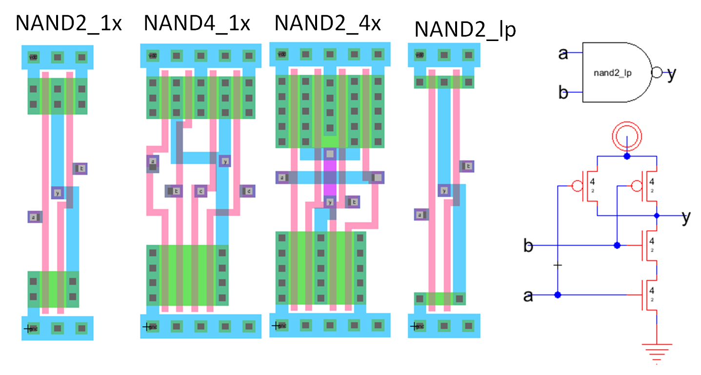
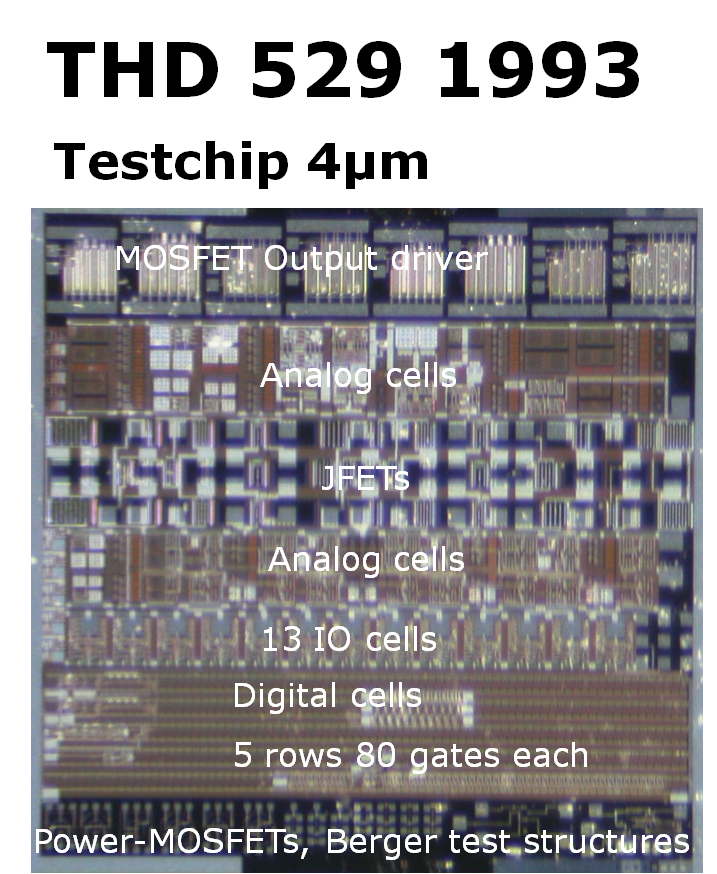
Cell Discussion:
Transistors
Width determined by number of input and outputs
Same height, names, vertical horizontal lines, exports, hierarchy
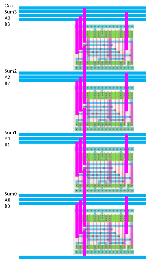
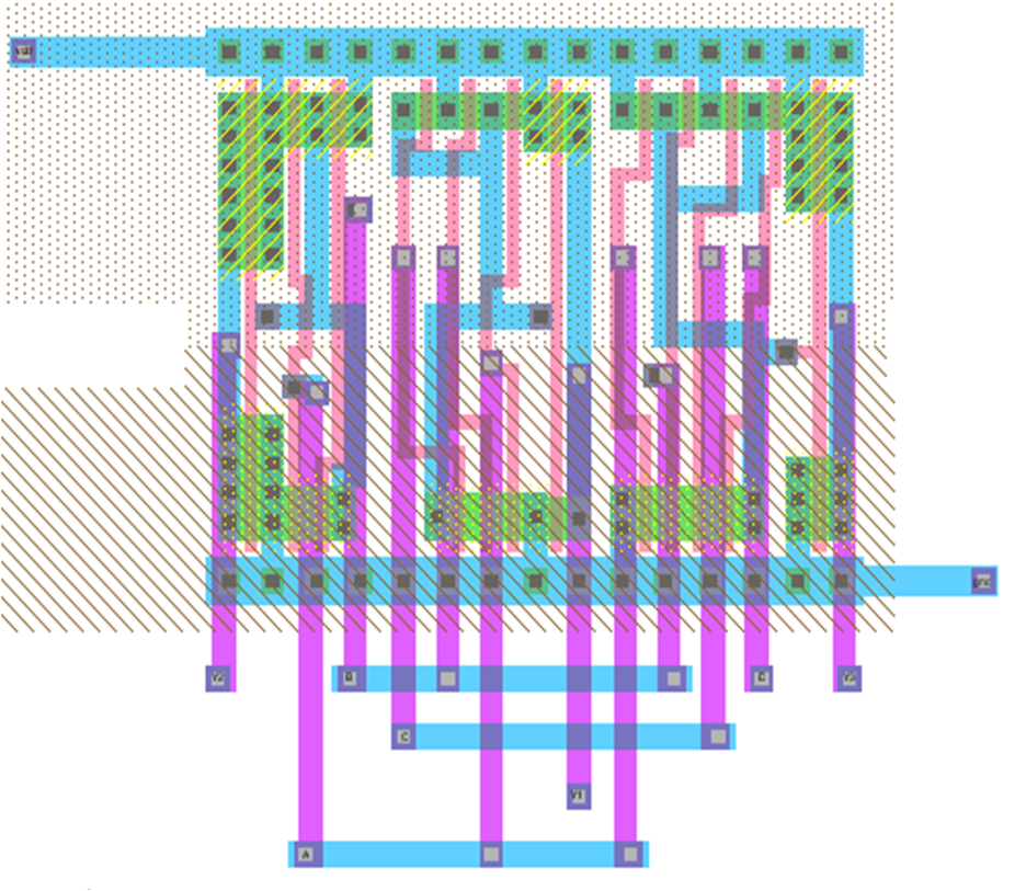
Layout 1-Bit Adder
library: muddlib_07
cell: fulladder
pins: a, b, cin, sum, cout
Very nice regular
Not area optimized
Standard cell
M2 used
Vertical pink
Polysilicon
Vertical
Evenly spaced
M1
horizontal
This is an example from a MIPS microprocessor.
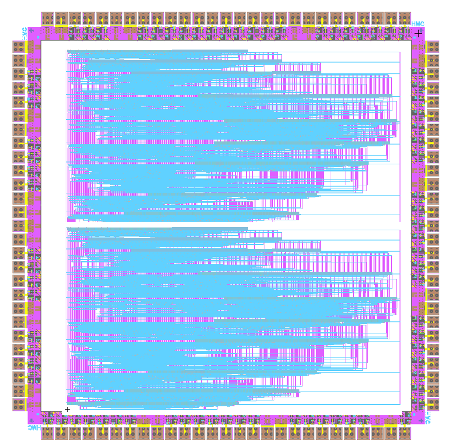
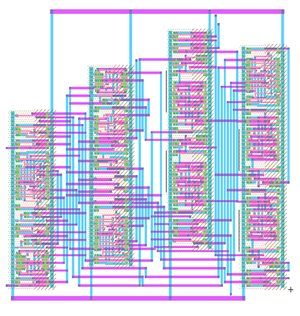
Multiple cells: 4 Bit Adder Floorplan
Use grid for wiring
Metal 1:
Horizontal
Metal 2:
Vertical
Cell input and output
Different x and y coordinates
Since Carry is propagated Cin and Cout have the same x coordinates
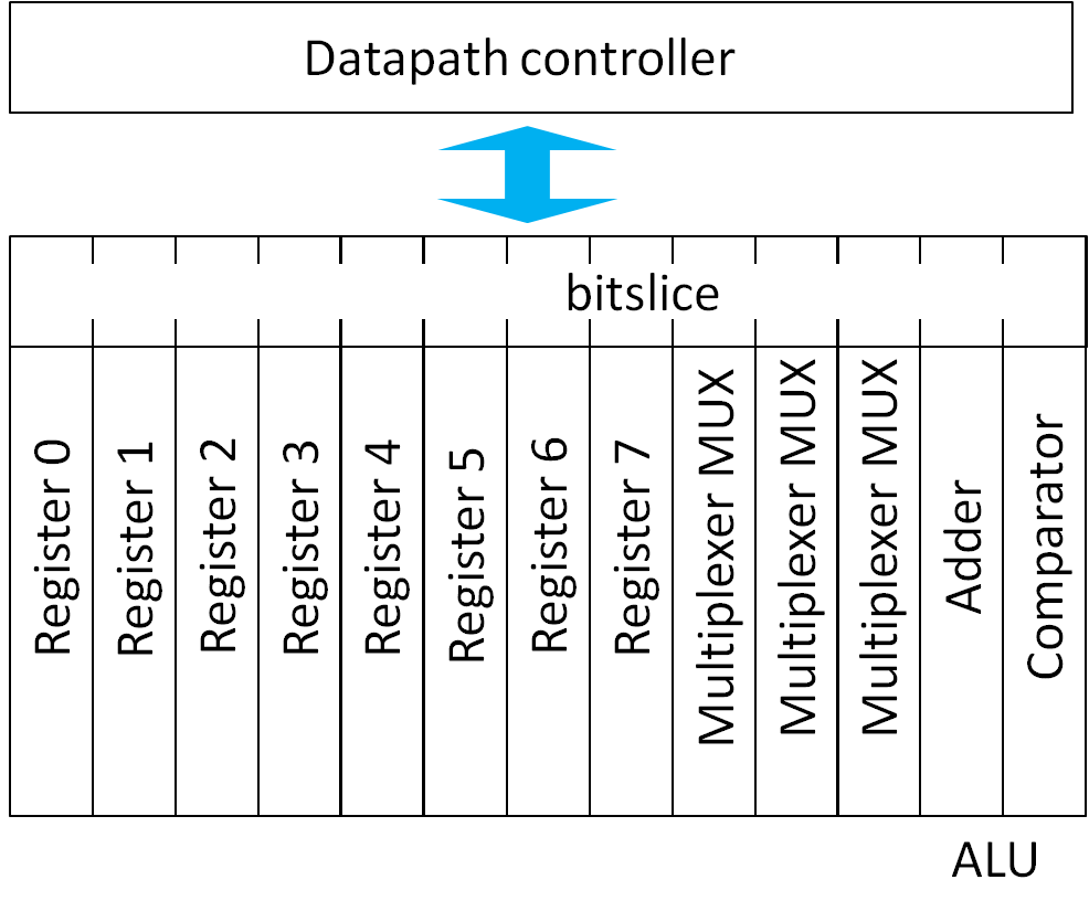
Manual planning, place and route for data path
Control circuits are at the top.
For each bit a row (bitslice) is taken with functionality of register, mux, alu.
Chip layout
Area is square to maximize area for a given number of pins at the edge.
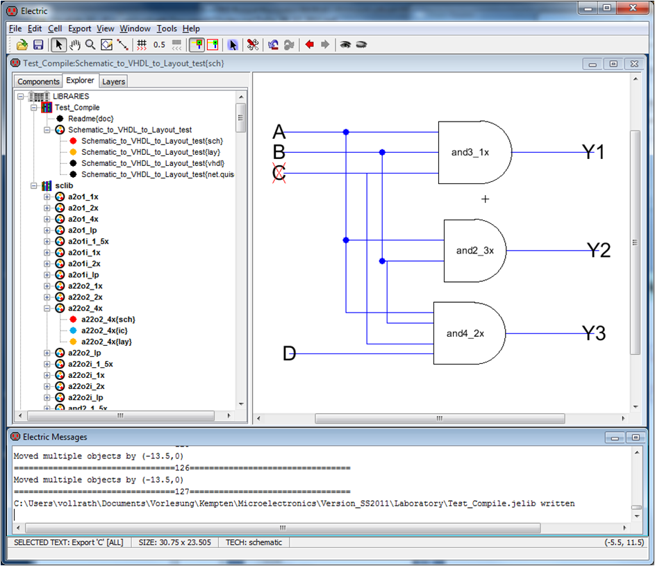
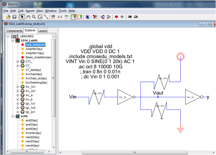
Design Entry
Schematic
Layout
Graphical State machine
VHDL
SystemC
C/C++
Schematic and VHDL
There are tools available to convert a schematic to layout.
This operation is called synthesis and in "VLSI Design System" a tool Silicon Compiler is used.
This tool needs basic layouts for transistors or logic cells which are available in sclib.jelib.
This library has to be loaded before using the Silicon Compiler.
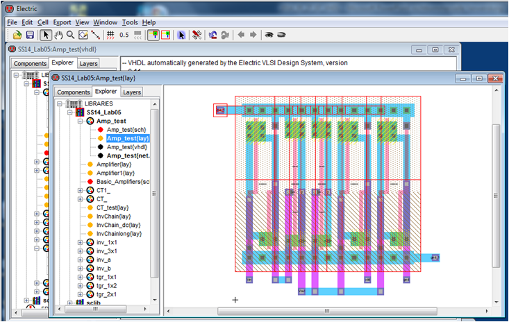
Here a schematic of a typical logic circuit is shown. Each logic circuits has a layout.
The Silicon Compiler places the layout cells and does the wiring using M1 and M2.
The next slides shows the result and more detailed instructions
to get the Silicon Compiler working without errors.
Engineering tools normally have some quirks and error messages and special procedures
to overcome errors. Bug fix requests are often done, but seldom implemented due
to successful workarounds.
A trained user will avoid these errors and stops complaining after a while.
An engineer should be aware of this and able to find workarounds.
Layout
The picture shows the generated layout.
The wiring of logic cells is done by routing M2 wires vertically below the cells
and connecting these wires with horizontally running M1 wires.
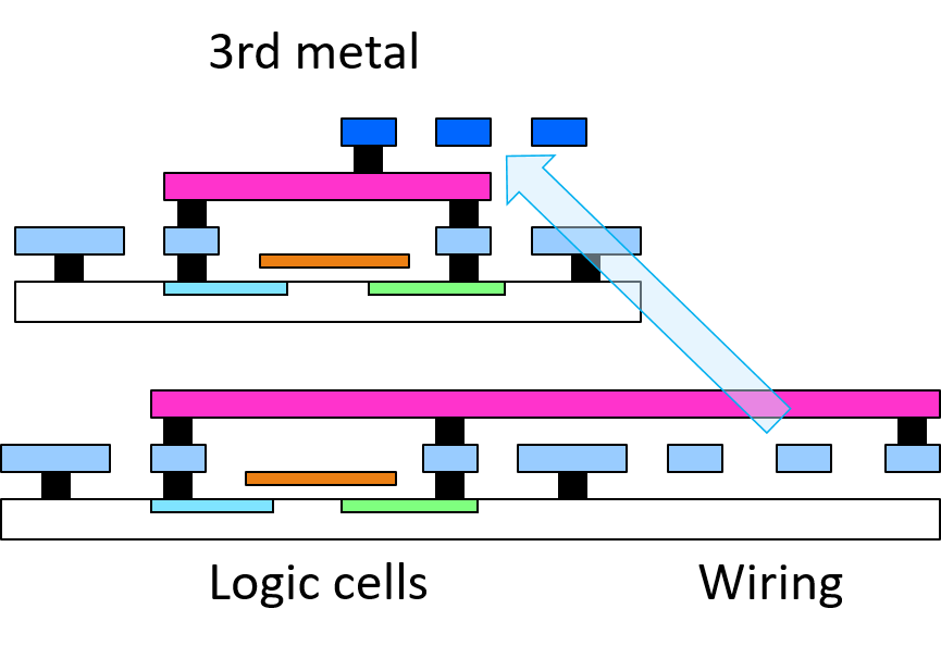
Wiring Layers and Area
On the left is a automatically placed and routed layout.
Light blue metal1 M1 lines are used vertically, M2 lines are used horizontally.
Between strips/columns of logic cells the M1, M2 routing is placed.
More area is used for wiring than for active devices.
Having more metal layers for routing allows putting wiring on top of logic cells.
This is shown on the cross section on the left side, where 2 M1 lines are placed
as M3 lines on top and the width of the layout is reduced.
The layout was generated using a mod_m_counter layout.
Silicon Compiler Start
Select a schematic
Tools->Silicon Compiler -> Convert current cell to layout
Sclib is opened
Vhdl, net view are created
Error message
Modify vhdl view
Delete entities of subcircuits
Copy these subcircuit groups including layout to sclib
Delete ground, power component in vhdl or create it and modify signal list.
VHDL code relating to cells with layout in sclib (LUT2, MUX, FDC)
having nmos, pmos subcircuit in it, should be deleted.
Connections to vdd or gnd have to be modified,
so that these are using vddx and gndx signals,
which will be connected at the top level to vdd and gnd.
Silicon Compiler Continued
Error message:
SC Maker cannot find Horizontal Arc Metal-1 in technology artwork
Select a metal arc in a layout
Select vhdl and do Silicon Compiler
Error: Exception
Change number of rows and try again
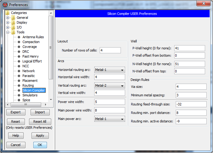
Preferences -> Tools -> Silicon Compiler
Number of rows
Routing min active distance -9
Horizontal spacing
Error:SC Maker cannot find Horizontal Arc Metal-1 in technology artwork
Select a metal arc in a layout
Then in Preferences, Tools, Silicon compiler, under Arcs:
Horizontal routing arc: Metal-1
Vertical routing arc: Metal-2
should appear.
Silicon Compiler Finish
Preferences -> Tools -> Silicon Compiler
Number of rows
Routing min active distance -9
Horizontal spacing
A new silicon compiler run will create another layout
Nothing will be lost
VHDL overview
What is VHDL?
Strategy: Copy, paste, adapt
Basic Block structure
Keywords
Hierarchy and Connection
State machine
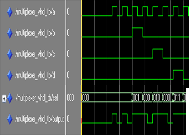
Test vector
Summary
You do not need to know all details of VHDL!
Copy, paste, modify
In former times a tool or programming language first was studied in detail
and then examples were programmed.
Nowadays there are many working examples or libraries available using good coding style,
good documentation and test benches.
Working examples are studied, copied, pasted and modified on a need to know basis.
VHDL examples should have the hardware code and a test bench with an expected output
to be able to verify operation and understand the circuit.
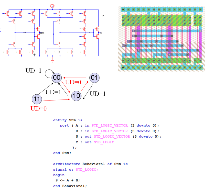
entity Sum is
   port ( A : in STD_LOGIC_VECTOR (3 downto 0);
          B : in STD_LOGIC_VECTOR (3 downto 0);
          S : out STD_LOGIC_VECTOR (3 downto 0);
          C : out STD_LOGIC
			 );
end Sum;

architecture Behavioral of Sum is
signal o: STD_LOGIC;
begin
 S <= A + B;
end Behavioral;
Ports, Busses and Signals
Input and Output of a circuit: Port
In The signal can only be read (right side of connection)
Out The signal can only be set (left side of connection)
Buffer The signal can be read and set.
Inout The signal can be read and set
assignment: Y<= ‘0‘;
Bus:
STD_LOGIC_VECTOR, BIT_VECTOR
MY_SHORT: in STD_LOGIC_VECTOR(3 downto 0);
MY_SHORT <= “ 1101“;
Individual Line: Y <= MY_WORD(2);
MY_WORD <= MY_SHORT_1 & A & B & C; a bus consisting of some signals.
Signal
signal Y1, Y2: bit;
Local lines can be set and read.
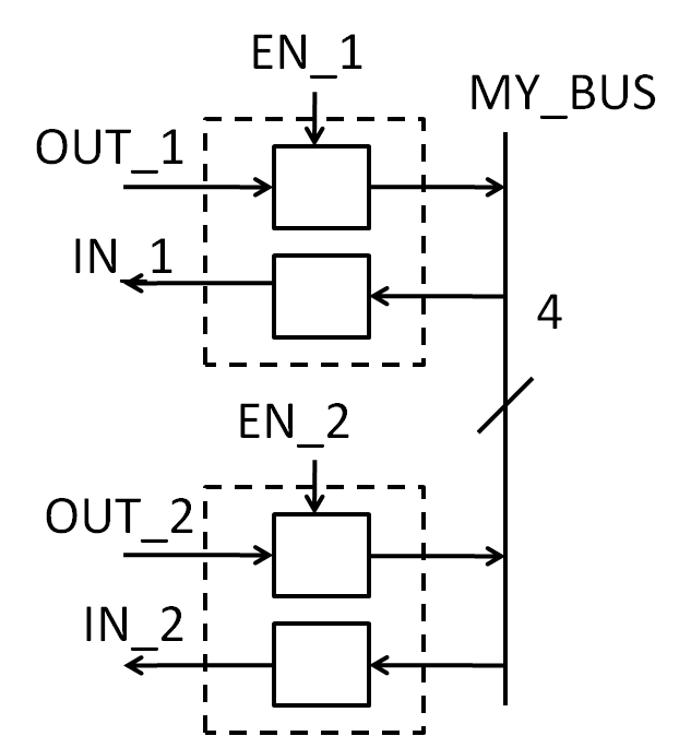
Three-state-driver
Buses are used to save lines.
Time muxed signals are transmitted.
The driver is enabled via EN signal and has otherwise the state ‘Z‘.
signal IN_1,OUT_1,IN_2, OUT_2, MY_BUS: std_logic_vector(3 downto 0);
Signal EN_1;EN_2:std_logic;
begin
IN_1 <= MY_BUS; IN_2 <= MY_BUS;
MY_BUS <= OUT_1 when EN_1= ‘1‘ else (others=>‘Z‘);
MY_BUS <= OUT_2 when EN_2= ‘1‘ else (others=>‘Z‘);
end Test;
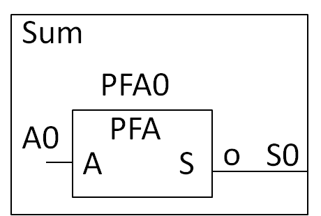
Hierarchy and Connection
Use components
State the port definition
Declare signals
Use Components
by naming instance
PFA0: PFA
By connecting input and outputs
Port map ( name of original port => local signal name
architecture Behavioral of Sum is
 component PFA
      port( A: in STD_LOGIC;
            S: out STD_LOGIC);
  end component PFA;
signal o: STD_LOGIC;
begin
PFA0: PFA
   port map (A=>A0, S=>o);
 S0 <= o;
end Behavioral;
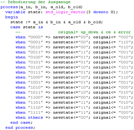
State machine, process, incomplete if
Process
Variable
Case statement
Truth table
Synchronous design
Rising edge
Register
Incomplete if statement
process (a_in, b_in)
 variable state: STD_LOGIC_VECTOR(1 downto  0)
Begin
 state := a_in & b_in;
 case state is
   when   "00" => newstate<= "0000";
   when   "01" => newstate <= "0100";
   when others => newstate <= "0100";
  end case;
End process;

-- transfer new state to old state
process (clk, newstate)
 begin
  if rising_edge(clk) then
     oldstate <= newstate;
  endif;
end process;
Finite state machine in VHDL
Truth table: logic
Register transfer
Library IEEE
Basic definitions for example:
STD_LOGIC
More Libraries available
Look for functions provided
Speeds up development process
library ieee;

use ieee.std_logic_1164.all;
use ieee.numeric_std.all;
Test and input signals
Constant
Process label
Wait for statement
-- Clock period definitions
   constant clk_period : time := 0.02us;
-- Clock process definitions
   clk_process :process
   begin
		clk <= '0';	wait for clk_period/2;
		clk <= '1';  wait for clk_period/2;
   end process;
    -- Stimulus process
   stim_proc: process
   begin
      -- hold reset state for 1us.
      wait for clk_period*50; -- 1us
      wait for clk_period*50; -- 1us
      A <= '0'; B <= '0';
      wait for clk_period*50; -- 1us
      A <= '0'; B <= ‚1';
    end process;
Input signal timing
procedure VECTORTIMING (CLKi,S1i,S0i: in std_logic) is
-------------------------------------------------------------------------------
-- timing information for usage with synchronous designs and test
-------------------------------------------------------------------------------
 constant TCYCLE : Time := 100ns;                      -- cycle time

 begin
    CLK <= CLKi after (TCYCLE/2), '0'after (TCYCLE);   -- CLK pulse width
    S1 <= S1i   after 10ns, '0' after 70ns;
    S0 <= S0i   after 10ns, '0' after 70ns;
    wait for TCYCLE;                                   -- go to cycle end time
end procedure VECTORTIMING;

Begin
--     VECTORTIMING (CLKi,  S1i,  S0i );
------------------------------------------------------------------------
       VECTORTIMING ( '1',  '1',  '0‘ );
End;
VHDL Design and Verification Environment
No cost
FPGA vendors: Altera, Xilinx
Xilinx WebPack free to download
Behavioral and structural VHDL
Behavioral
entity mod_m_counter is
   generic(
      N: integer := 4;     -- number of bits
      M: integer := 10     -- mod-M
  );
   port(
      clk, reset: in std_logic;
      max_tick: out std_logic;
      q: out std_logic_vector(N-1 downto 0)
   );
end mod_m_counter;

architecture arch of mod_m_counter is
   signal r_reg: unsigned(N-1 downto 0);
   signal r_next: unsigned(N-1 downto 0);
begin
   -- register
   process(clk,reset)
   begin
      if (reset='1') then
         r_reg <= (others=>'0');
      elsif (clk'event and clk='1') then
         r_reg <= r_next;
      end if;
   end process;
   -- next-state logic
   r_next <= (others=>'0') when r_reg=(M-1) else
             r_reg + 1;
   -- output logic
   q <= std_logic_vector(r_reg);
   max_tick <= '1' when r_reg=(M-1) else '0';
end arch;
Structural
entity LUT4_0DF0 is port( I0,I1,I2,I3: in STD_LOGIC;O: out STD_LOGIC);
end LUT4_0DF0;

architecture LUT4_0DF0_BODY of LUT4_0DF0 is
  component LUT20 port ( I0,I1 : in STD_LOGIC;O: out STD_LOGIC); end component;
  component LUT2D port ( I0,I1 : in STD_LOGIC;O: out STD_LOGIC); end component;
  component LUT2F port ( I0,I1 : in STD_LOGIC;O: out STD_LOGIC); end component;
  component MUX4 port(I0,I1,I2,I3,I4,I5 : in STD_LOGIC;O: out STD_LOGIC); end component;

  signal y1,y2,y3,y4,O2 : STD_LOGIC ;

begin
  LUT2_1: LUT20 port map (I0,I1,Y1);
  LUT2_2: LUT2F port map (I0,I1,Y2);
  LUT2_3: LUT2D port map (I0,I1,Y3);
  LUT2_4: LUT20 port map (I0,I1,Y4);
  MUX0: MUX4 port map (Y1,Y2,Y3,Y4,I2,I3,O);
end LUT4_0DF0_BODY;
ISE Webpack can be used to transfer behavioral VHDL in structural VHDL. AnalyzeJS.html transfers the structural VHDL to Electric compatible VHDL.
Electric can then synthesize the circuit with elements of circuit sclib.jelib.
An example is synthesis of a UART.
Vivado can be used to transfer behavioral VHDL in structural VHDL.
After Synthesis run a command in the 'Tcl Console':
write_vhdl <filename>
A VHDL file using UNISIM components is generated.
A very basic FPGA like Arty S7-25 (xc7s25csga324-1) should be used to limit the
variety of UNISIM components.
(FDRE, IBUF, OBUF, LUT1, LUT6, BUFG, LUT2, LUT3, LUT4, LUT5, LUT6, CARRY4)
Summary VHDL
Block description:
Entity, Architecture
Interface (port, in, out, inout) and wires (signal)
Std_logic, std_logic_vector
Logic function
Connection y <=a
Boolean function: y <= a & b;
State machine
Truth table: Process, case, if
Edge triggered: Rising_edge(clk)