| Hierarchy | Memory | Cost per Bit | Speed | Density |
| L1 Cache | SRAM |
highest

lowest
|
fastest
slowest
|
32 kB; 128kB |
| L2 (L3) Cache | SRAM |
512 kB; 512kB (4MB) |
| Main Memory | DRAM |
16 GB; 4..64 GB |
| Flash Memory (SD Card) | NAND |
4 GB; 16 GB..1 TB |
| Hard Disk Memory | Magnetic/Flash |
4 TB/2..16 TB |
Cache: Intel Celeron (Core) 2007; Intel Core i3-7300 (Kaby Lake, 2017, 14nm)
Memory Types
DRAM (capacitor)
SRAM (latch of transistors)
Flash (transistor with floating gate)
FRAM (Ferro Electric hysteresis)
MRAM (Resistance change due to magnetization)
PCRAM (resistance change due to solid/solid transition)
- Word in bit
- Memory capacty in bit (b) oder byte (B):
k(ilo) =210 =1024, M(ega) = 220 =1048576,
G(iga) = 230 , T(era)=240, P(eta)=250
- Power consumption
- Access time
- Write time
- Data Retention
- Endurance
Needed Area
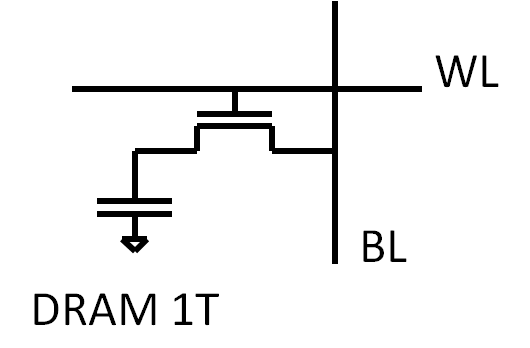
DRAM: 6F 2 one capacitor + 1 select device: 1T + capacitor
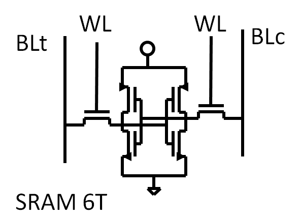
SRAM: 256F 2 4 transistors + 2 select devices: 6 T
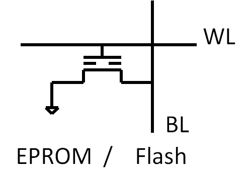
Flash: 4F 2 (16 level: 1F 2) 1 Transistor with floating gate: 1T
Volatile versus nonvolatile memories
Information loss: Volatile versus nonvolatile memories
SRAM, DRAM lose information without power, Flash, EPROM and FRAM donÆt.
DRAM loses information without constant refresh of memory cells.
Memory Array
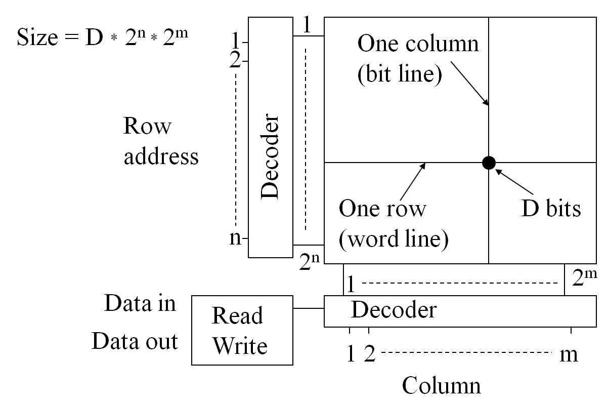
Activation:
Lets analyze a typical DRAM from Micron, Samsung, Hynix.
Biggest size DRAM datasheet from Internet.
Number of outputs, row address, column address, banks.
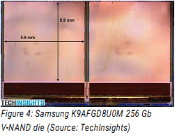
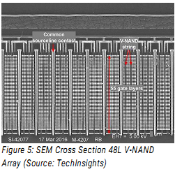
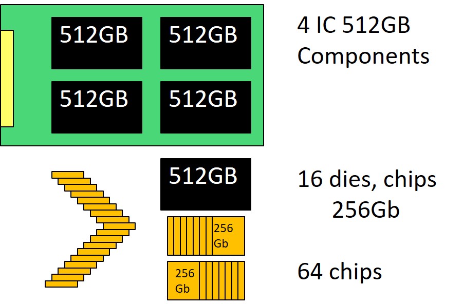
Samsung 21nm 48L V- 256Gb NAND Flash memory in 2TB SSD
- 7.4.2016 EE Times
- 256 Gb Chip: 3 bit per cell
- 512 GB K9DUB8S7M Component
= 8*512 Gb -> 16*256Gb
- 2 TB solid state drive (SSD)
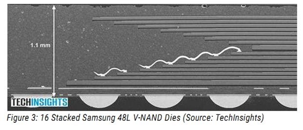
- 16 Chips (dies) 40um Thick
- Die area: 100mm2
|
|
|
|
The density is not only determined by F, but by the number of bits ber cell(3) and
vertical integration (48 layers of transistors, 16 dies)
Multiple bits per cell.
Multiple cells stacked vertically.
Multiple chips per package.
More functionality per volume.
Memory Array SRAM
Positive clock level control
CLK AND (A1, A0) selects a row
CLK AND (A2, A3) selects a column
WE AND CLK connects DI with data lines
Where is the memory cell with address (A3..A0) = "0110"?
Which switches are closed with address (A3..A0) = "0110"?
Memory cells are connected to BL and BLb.
BL and BLb are equalized with CLK='0'
Simulation
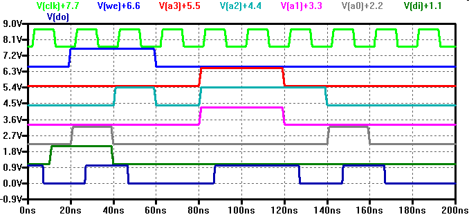
Positive clock level control
Read 0000 '0', Read 0001, Write 0001 æ1æ, Write 0100 æ0æ, Read 0000 '0',
Read 1110 '1', Read 1110 '1', Read 0100 '0', Read 0001 '1', Read 0000 '0', Read 0000 '0'
Delay 10ns from address until data appears
VHDL-Code: ROM
library ieee;
use ieee.std_logic_1164.all;
use ieee.numeric_std.all;
entity ROM_INSTANZIIERUNG is
   generic(ADDR_RANGE: integer:=4;
           DATA_WIDTH: integer:=8);
   port (ADDRESS : in std_logic_vector(ADDR_RANGE-1 downto 0);
         DATA : out std_logic_vector(DATA_WIDTH-1 downto 0));
end ROM_INSTANZIIERUNG;
architecture VERHALTEN of ROM_INSTANZIIERUNG is
type ROM_TYPE is array (0 to 2**ADDR_RANGE -1) of std_logic_vector(DATA_WIDTH-1 downto 0);
constant ROM : ROM_TYPE :=
   (x"0F",x"0E",x"0D",x"0C",x"0B",x"0A",x"09",x"08",
	 x"07",x"06",x"05",x"04",x"03",x"02",x"01",x"00");
begin
   DATA <= ROM(to_integer(unsigned((ADDRESS)));  -- Lesezugriff
end VERHALTEN;
VHDL-Code: RAM 01
entity Xilinx_one_port_ram_sync is
  generic(
    ADDR_WIDTH: integer :=12;
    DATA_WIDTH: integer:=8
   );
  port (
      clk: in std_logic;
      we: in std_logic;
      addr: in std_logic_vector(ADDR_WIDTH-1 downto 0);
      din: in std_logic_vector(DATA_WIDTH-1 downto 0);
      dout: out std_logic_vector(DATA_WIDTH-1 downto 0)
    );
end Xilinx_one_port_ram_sync;

Ram_1K_by_16_0: entity Xilinx_one_port_ram_sync
  generic map(ADDR_WIDTH=>10;DATA_WIDTH=>16)
  port map(clk => clk, we=>we,addr=>addr,din=>din,dout=>dout);
VHDL-Code: RAM 02
architecture Behavioral of Int_Memory is
type ram_type is array (2**ADDR_WIDTH-1 downto 0) of
std_logic_vector (DATA_WIDTH-1 downto 0);
signal ram: ram_type:= (others => (others => '0'));
Begin
process(clk)
begin
if ((clkæevent) and clk=æ1æ) then
if (we =æ1æ) then
ram(to_integer(unsigned(addr))) <= din;
end if;
dout <= ram(to_integer(unsigned(addr)));
end if;
end process;
end Behavioral;
DDR3 SDRAM Access
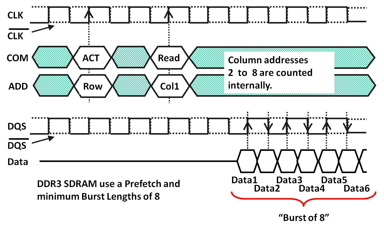
Cycle time:
Latency:
Summary
- Memory as data and program buffer
- SRAM, DRAM, ROM, NAND flash memory
- Capacity, (non)volatile, latency, bandwidth
- Memory array: realization, layout, LTSPICE, VHDL
- Memory access timing
Next: 12 Power, Clock, Input, Output (IO)
|
