Open Laboratory 5, 2017: Synthesis and design exploration of an ALU
Jörg Vollrath
This practical training looks at challenges in synthesis of digital circuits.
Synthesis of a VHDL circuit with Electric
Study the steps involved in synthesizing a UART.
Synthesis of a UART from VHDL to Chip
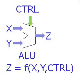
A 4-Bit ALU
A 4-Bit ALU is designed and synthesized step by step from VHDL.
- Generate VHDL for a 4-Bit Adder Z = X + Y
- Simulate and synthesize a 4-Bit Adder
- Measure area, power consumption and maximum clock rate of the 4-Bit adder with RCX.
- Add the operations: Subtract Z=X-Y, set carry flag C=0
- Add the operations: shift X one bit left, shift X one bit right
- Add the boolean operations: AND, OR, INV X
- Extension:
- Optimize Electric VHDL code
- Replace a MUX4 cell with an optimized MUX4 cell.
Study the increase in area, circuits, complexity and simulation time with and without RLC yes/no (parasitics).
Tool chain
A VHDL description of a 4-Bit ALU is mapped to logic blocks using Xilinx ISE webpack.
The VHDL description is modified for Electric VLSI system using AnalyzeJS.js.
A standard cell library sclib.jelib is used with VHDL code to synthesize a 4-Bit ALU.
Adder VHDL
Start ISE WEbpack and create a new project with ALU VHDL code.Select File -> New Project; Set Name: "ALU"; Top-level source type should be HDL; Next;
Project Settings: Family Spartan3E; Device: XC3S250E; Package CP132; Preferred Language: VHDL; Next; Finish
In the Design tab Hierarchy window (top-left) right click mouse and New Source:
use IEEE.std_logic_arith.all;
...
entity Adder4Bit is
    Port ( A : in  STD_LOGIC_VECTOR (3 downto 0);
           B : in  STD_LOGIC_VECTOR (3 downto 0);
           CLK : in  STD_LOGIC;
			  RESET : in  STD_LOGIC;
           CIN : in  STD_LOGIC;
           Y : out  STD_LOGIC_VECTOR (3 downto 0);
           COUT : out  STD_LOGIC);
end Adder4Bit;

architecture Behavioral of Adder4Bit is
signal YX: STD_LOGIC_VECTOR (4 downto 0);
signal AI: STD_LOGIC_VECTOR (4 downto 0);
signal BI: STD_LOGIC_VECTOR (4 downto 0);
signal CI: STD_LOGIC_VECTOR (4 downto 0);

begin
 AI <= '0' & A;
 BI <= '0' & B;
 CI <= "0000" & CIN;
    process(clk,reset)
     begin
       if ( reset = '1') then
            YX <="00000";
       elsif  (clk'event) and (clk='1') then
	         YX <= unsigned(AI) + unsigned(BI)
				      + unsigned(CI);
       end if;
     end process;
 Y <= YX(3 downto 0);
 COUT <= YX(4);
end Behavioral;
Create VHDL for synthesis of a layout
In the Design tab choose View: Implementation.In the Process window (center-left) open the submenu of Synthesize - XST by clicking on the plus sign and start the process Generate Post-Synthesis Simulation Model.
This creates a structural VHDL code file in a subfolder: netgen/synthesis/adder4Bit_synthesis.vhd
This file will be used later for synthesis of a layout.
Simulate behavior
In the Design tab choose View: Simulation.In the 'Design' tab Hierarchy window (top-left) right click mouse and do 'New Source'.
Select 'VHDL Test Bench' and 'File name': test_adder4; Next; Adder4Bit; Next; Finish;
Open test_adder4 file with a double click.
There is a section '-- insert stimulus here' and apply the reset signal for 100 ns.
      -- insert stimulus here

      wait for clk_period*10;

      reset <= '0'; wait for 100 ns;
      reset <= '1'; wait for 100 ns;
      reset <= '0'; wait for 100 ns;
Select test_adder4.In the Process window (center-left) open the submenu of ISIM Simulator by clicking on the plus sign and start 'Simulate Behavioral Model'.
ISim is starting and the signals are displayed.
Document the results.
Process VHDL
Start AnalyzeJS.html to be able to process Xilinx VHDL. Copy your netgen/synthesis/adder4Bit_synthesis.vhd file into the input box.Press 'Update source and process it'.
Open Electric VLSI Design System.
Open library sclib.jelib
Create new cell: View: VHDL; Name Adder4Bit.
Copy the "Entities" section from AnalyzeJS into the window.
Copy from "Processed output" section starting with line entity from AnalyzeJS into the window below the entities.
After the line "architecture Structure of Adder4Bit is" and before signal copy the section "Components" from AnalyzeJS.
Modify the presets of clk and reset in the entity.
Remove ; after last port.
If there are entities FDC0 or LUT12:
Remove entity FDC0 since it is not used.
Remove entity LUT12 and replace LUT12 usage with IBUF.
Synthesize Circuit and Simulate
Select M1 in another cell to enable the right layers for routing.Select adder4Bit{vhdl}.
Tools-> Silicon Compiler -> Convert current cell to layout.
For simulation create a new cell adder4Bit_doc.waveform.
In the tab 'Components' place the cell adder4Bit layout.
Add the LTSPICE simulation text:
.include cmosedu_models.txt
VGND Adder4Bi@0_gnd 0 DC 0
VDD Adder4Bi@0_vdd 0 DC 1
VA0 Adder4Bi@0_A__0 0 PULSE(0 1 10n 1n 1n 9n 20n)
VA1 Adder4Bi@0_A__1 0 PULSE(0 1 30n 1n 1n 9n 20n)
VA2 Adder4Bi@0_A__2 0 PULSE(0 1 50n 1n 1n 9n 20n)
VA3 Adder4Bi@0_A__3 0 PULSE(0 1 70n 1n 1n 9n 20n)
VB0 Adder4Bi@0_B__0 0 PULSE(0 1 90n 1n 1n 9n 20n)
VB1 Adder4Bi@0_B__1 0 PULSE(0 1 110n 1n 1n 9n 20n)
VB2 Adder4Bi@0_B__2 0 PULSE(0 1 130n 1n 1n 9n 20n)
VB3 Adder4Bi@0_B__3 0 PULSE(0 1 150n 1n 1n 9n 20n)
VCIN Adder4Bi@0_CIN 0 PULSE(0 1 1000n 1n 1n 9n 2000n)
VCLK Adder4Bi@0_CLK 0 PULSE(0 1 15n 1n 1n 9n 20n)
VRST Adder4Bi@0_RESET 0 PULSE(0 1 10n 1n 1n 9n 2000n)
.tran 2000ns
Do a LTSPICE simulation to check functionality.
Since the top level cell needs some inputs check that the voltage source names match inputs and outputs of the topmost cell.
*** TOP LEVEL CELL: Adder4Bit_Test{lay}
XAdder4Bi@0 Adder4Bi@0_A__0 Adder4Bi@0_A__1 Adder4Bi@0_A__2 Adder4Bi@0_A__3
+Adder4Bi@0_B__0 Adder4Bi@0_B__1 Adder4Bi@0_B__2 Adder4Bi@0_B__3
+Adder4Bi@0_CIN Adder4Bi@0_CLK Adder4Bi@0_COUT Adder4Bi@0_RESET
+Adder4Bi@0_Y__0 Adder4Bi@0_Y__1 Adder4Bi@0_Y__2 Adder4Bi@0_Y__3
+Adder4Bi@0_gnd Adder4Bi@0_vdd Adder4Bit
Document your simulation result.
Repeat simulation with RCX extraction.
Synthesize an ALU
New functionality will be added step by step. It is not clear how much functionality can be added during this laboratory (Open laboratory).Start with Step 1 and do the synthesis, simulation and documentation. Then proceed.
Create a new Cell after each Step, so you don't loose your previous work.
- Add the operations: Subtract, set carry flag 0, implement zero flag
- Add the operations: shift one bit left, shift one bit right
- Add the boolean operations: AND, OR, INV
- Extension:
- Optimize Electric VHDL code
- Replace a MUX4 cell with an optimized MUX4 cell.
Study the increase in area, circuits, complexity and simulation time with and without RLC yes/no (parasitics).
Extension: Optimize VHDL code and the cells for a LUT4 table
Investigate the used LUT4 and LUT2 circuits and replace at least one of them with an improved layout according to the rules in the class.Investigate the structural VHDL. Can you optimize the VHDL code?
How much improvement in area, power consumption and maximum clock frequency can you achieve?
Document your results.
Deliverables
Document your laboratory in a pdf document with a name of < Date > _2017_ALU_ < name > .pdf and send it to joerg.vollrath@hs-kempten.de.A maximum of 2 students can prepare a document together clearly marking authorship of different sections. Submission is due 7.7.2017.
- ALU VHDL code
- Electric VHDL code
- ISIM Simulation of ALU VHDL code
- < Name > .jelib with alu layout and simulation code
- LTSPICE RCX simulation netlist of one layout
- LTSPICE simulation result
- Maximum delay
- Power consumption at various clock frequencies
- Table with area, power consumption, maximum clock speed of counters