Microelectronics
Feedback
Prof. Dr. Jörg Vollrath |
|
Laboratory 3/4
Discuss the statement:
Those inverters, which are mostly built by PMOS transistors,
have worse electrical characteristics than those which mainly
consist of NMOS semiconductors due to switching losses which are remarkable
higher at PMOS structures.
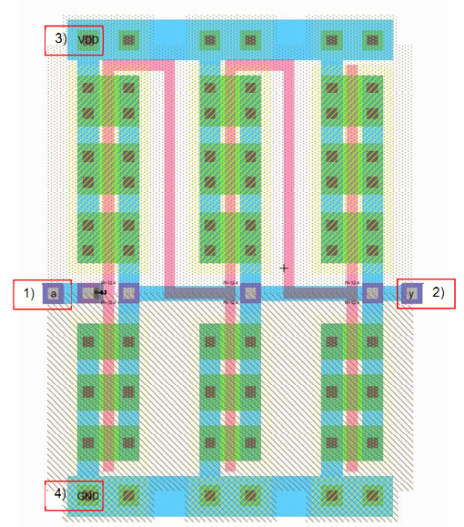
Polysilicon can go under M1 without short.
A short connection in the center could be used.
Why are the exports (M2 contacts) stretching beyond width of cell?
Precision of measurement
1.16 ns - 1.13ns =
More digits are needed.
0.34534 ns
It can be an interpolated value: 2..3 digits accuracy.
Polysilicon delay only active with conservative RC.
Open questions: ambiguity
How much time did you spent?
Detail, report writing, laboratory hours, tasks
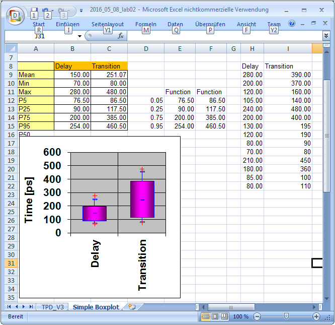
Laboratory 3/4 Data processing
- Log file:
prop_vout5_vout7: t_vout7_50-t_vout5_50=3.15337e
t_vout8_50: v(vout8)=v(vdd)/2 AT 1.33912e
- Table
- line plot
- Box plot:
min, max, average(Mittelwert), 5,25, 50,75,95 percentile (quantil)
Boxplot.xlsx
|
|
Laboratory 3/4 Data processing
- Log file:
prop_vout5_vout7: t_vout7_50-t_vout5_50=3.15337e
t_vout8_50: v(vout8)=v(vdd)/2 AT 1.33912e
- Table
- line plot
- Box plot:
min, max, average(Mittelwert), 5,25, 50,75,95 percentile (quantil)
Boxplot.xlsx
|
|
Reflection and Learning
- This is the schematic, layout and measurement result
-
- By copy paste doing schematic is easy. Error message analysis is useful.
NFET, PFET ratio shifts the transfer curve. -
- What is the intention?
What did I learn?
What was good?
What needs improvement? -
- Continous learning
Intention of a laboratory report
- Provide all information to be able to redo the laboratory and get same results
Problems and solutions should be listed
All files have to be listed in the text, in appendix or provided as link.
- Provide a short summary about the results
A transfer curve gives threshold voltage and maximum current.
This verifies the transistor performance.
Effective searches can be done using good headings and summaries.
- Discussion of results
This higlights the understanding of the student about the subject enabling the
teacher to give additional information and teaching.
Electric SS2022
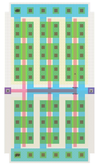
- Well resizing: Blue arrow activate/deactivate special select
Inverter, 2 contacts, well width 24
- Layout: Export vdd, gnd as power to enable Silicon Compiler power wiring
Synthesis with Silicon Compiler
Problem: layout of power can not have exports vdd twice
Solution: change exports to gndx, vddx and use these in VHDL
Before
-------------------- Cell LUT23{sch} --------------------
entity LUT23 is port(I0, I1: in BIT; O: out BIT);
  end LUT23;

architecture LUT23_BODY of LUT23 is
  component ground port(gndx: out BIT);
    end component;
  component nMOStran port(g: in BIT; s, d: inout BIT);
    end component;
  component PMOStran port(g: in BIT; s, d: inout BIT);
    end component;
  component power port(vddx: out BIT);
    end component;

  signal gndx, vddx: BIT;

begin
  gnd_0: ground port map(gndx);
  nmos_1: nMOStran port map(I1, gndx, O);
  pmos_0: PMOStran port map(I1, O, vddx);
  pwr_0: power port map(vddx);
end LUT23_BODY;
After
-------------------- Cell LUT23{sch} --------------------
entity LUT23 is port(I0, I1, vddx, gndx: in BIT; O: out BIT);
  end LUT23;

architecture LUT23_BODY of LUT23 is
  component nMOStran port(g: in BIT; s, d: inout BIT);
    end component;
  component PMOStran port(g: in BIT; s, d: inout BIT);
    end component;

begin
  nmos_1: nMOStran port map(I1, gndx, O);
  pmos_0: PMOStran port map(I1, O, vddx);
end LUT23_BODY;
Laboratory 2022 Boxplot
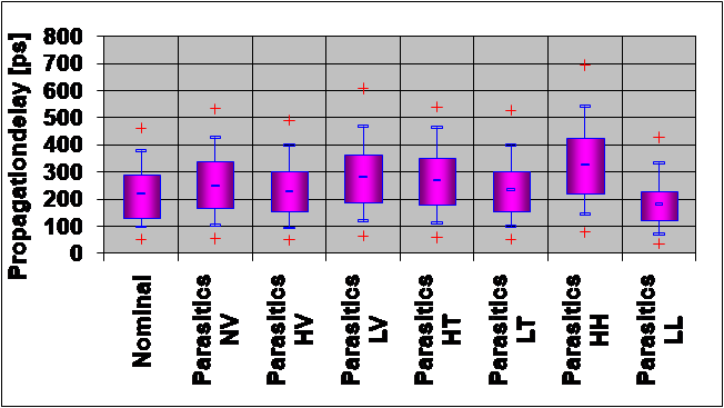
In microelectronics experiments are done for robustnest, resilence of circuits.
Typically one parameter (like length) is varied and the result ist studied.
The graph shows the influence of voltage (HV high voltage, NV nominal voltage, LV low voltage),
temperatur (HT high temperature, LT low temperature) and parasitics on propagation delay.
High voltage reduces propagation delay.
High temperature increases propagation delay.
Parasitics increase propagation delay.
Propagation delay is between 200ps and 300ps.
The boxplot shows min, max, percentiles and average values.
Sometimes also individual values are shown as points.
Wikipedia Boxplot
Laboratory 2022 Be specific
Conclusion
After this lab we find out how to make a 9*1 inv and how to run
simulation in invchaindc and ivnchainlong. Also we find out the
way to calculate propagation delay and transition time.
Conclusion
After successful completion of the lab now we can analyze the propagation delays
for cascading inverters with varying width. We can also observe the different delays
due to different stage load and driver. Also, delays are different for the rising and
falling edges of the input. The transition time shows us the rise time and fall time
and we can compare the results.
Specific Conclusion
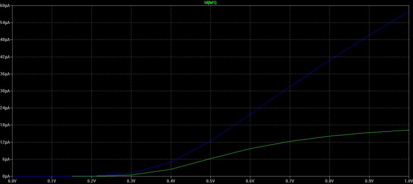
Static IV and dynamic curves (transient, propagation delay) of 50nm CMOS
inverters at 1V and room temperature varying NFET PFET ratio and
size with and without parasitic RC were studied.
VLSI Design system and LTSPICE were used for layout and simulation.
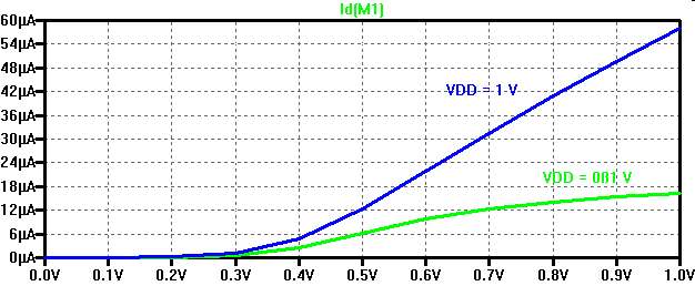
NFET PFET imbalance of a factor of 3 shift the static IV curve by 150 mV.
Smaller transistors, large loads and RC parasitics lead to propagation
delay variations from 17 ps to 56 ps.
Laboratory 2022 Questions
- What are good references?
- How to cite?
- What should be in the report?
- Should I show a LTSPICE netlist?
How should I display it?
- What do I expect the reader to take away?
Laboratory 2022 Comments
- Use IEEE format
- Sometimes only curves were shown,
no Vth and IDSmax was extraxted.
A summary table was missing
- Whole screen copy gives very small pictures.
Copy of a small window with 'Alt' 'print' can give better results
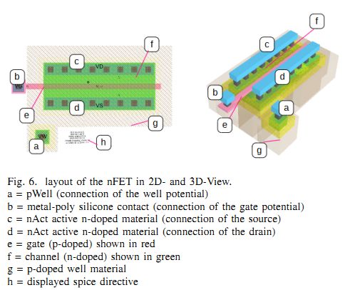
- Explain why you did a 3d view. What can be seen?
- In the text should be rferences to shown figures.
- Questions for summary and report(reflexion): What was learned?
- References: web page lab instructions, pdf, LTSPICE, VLSI tool, Baker book model, IEEE template
2019 Laboratory 1/2
Text
- Goal: Minimum time, effort and maximum result
What did you learn? Can you do now more? Reflection?
- Missing results:
Duration, summary table, text describing work
At the end: Did you answer all questions?
- Graph comments:
x-axis. y-axis. shape of curve, important parameters
- Expectations versus results
- Process description versus outcome description.
Step by step versus goal oriented.
- Why did you do something?
NCC highlighted differences between layout and schematic: label of pin exports
What is a good text?
Writing a typical IEEE publication of 8 pages, having all results and storyboard available, takes
at least 4h per page.
Laboratory 2018
- PFET section seems to be a copy and paste of NFET section.
PFET needs negative threshold voltage
Polarity of currents depends on measurement direction
- Software did not work well
What is better or worse than other engineering software
for example Matlab or Multisim?
- Plan in advance: Laboratory could be closed. Hard drive could crash.
Monday at laboratory: closed, did at home.
- Make a summary table
- Sloppy text: 1 µm instead of 50 nm, right instead of left, misspelling
- Listed LTSPICE code gives L, W and mosfet model,
therefore evaluation of results is possible.
- Black and grey background are bad
Laboratory 2018 (2)
- Sometimes only curves were shown,
no Vth and IDSmax was extraxted.
- Whole screen copy gives very small pictures.
Copy of a small window with 'Alt' 'print' can give better results
- Explain why you did a 3d view. What can be seen?
- Questions for summary and report(reflexion): What did I learn?
- Outdated instructions?
- Problem description should be precise and clear.
Not like:
We came to know that it requires some additional
settings which we must have to do in the electric for the successful
simulation.
Graphs
Black background, small font
White background, small font
Best:
White background, large font (small window), extra text
Plot Settings, Notes & Annotation
Plot with thick lines
|
|
3 D Graph
Best:
Picture with reference numbers for explanation
|
|