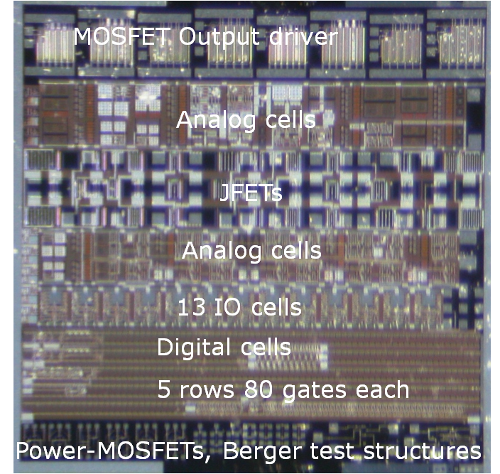
2020 Microelectronics |
||
|
This year the class is probably only online. General Remarks: Precise wording, description of errors helps finding solutions. Screen copies <Strg><Print/Druck> help. Text copies of LTSPICE netlists or error messages help. |
|
Questions:
Question:
I have a question regarding MOSFET Layout. Can you explain what the colors represent.
Different colors represent different materials or doping.
Orange/pink is polysilicon gate material.
Light green/blue are source drain doped regions.
Blue/violet are metal lines.
Black squares are contacts.
Question:
Unfortunately i still have a problem with the VLSI language since it is the first time i am dealing with this software, have you please documentation of VLSI software language (i can find only doc for transistor technology).
Answer:
Electric and LTSPICE are software tools. LTSPICE uses a netlist for circuit simulation.
Updated video:
Video Introduction 24.03.2020
Video LTSPICE and Electric 25.03.2020
Tutorials
http://cmosedu.com/videos/electric/electric_videos.htmQuestion:
I tried to simulate the my PFET layout that i have designed and found that i did something wrong.
WARNING: no power connection for P-transistor wells in cell Lab01_1u_00:PFET_1u_IV{lay}.
*** TOP LEVEL CELL: PFET_1u_IV{lay}
Mpmos@0 pmos@0_diff-bottom VG VD vdd P L=0.4U W=4U AS=37.5P AD=32.5P PS=27.5U
+PD=26.5U

* Spice Code nodes in cell cell 'PFET_1u_IV{lay}'
VSG 0 VG DC 0
VSD 0 VD DC 2
VBS VB 0 DC 0
VGND VS 0 DC 0
.include cmosedu_models.txt
.dc VSG 0 2 1m VBS 0 5 1
.END
pmos@0_diff-bottom: floating node, nothing connected.P: transitor model wrong. should be P_1u
vdd: floating node. Needs a voltage source attached.
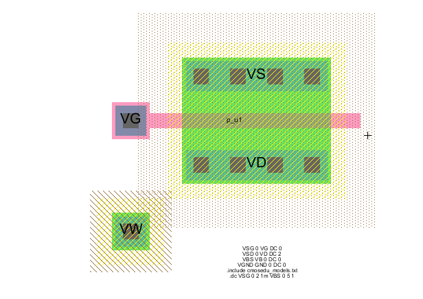
As you can see on the background pattern of the contact this is different then the background pattern of the transistor.
You are using the wrong contact. For a PFET you need a nwell contact.
Question:
I can not name the PMOS transistor model.
Answer:
Electric:
Model: select the transistor
Tools, Simulation (SPICE), Set Spice Model
text appears at the transistor SPICE model.
Question:
Electric Error:
Minimum width/height error((X axis)): cell 'PFET_1u_IV{lay}' node Metal-1-N-Well-Con['well@0'], layer 'N-Well' LESS THAN 12 WIDE (IS 11) [rule '1.1 Mosis, SUBM']
Answer:
Just make the n-well-contact bigger 6x6