▄bungsaufgabe: Erstellung einer Wahrheitstabelle und eines Signalverlaufes aus einer VHDL Beschreibung
Lõnge: 10:47 min
0:40 Wahrheitstabelle: Eingõnge, Ausgõnge
1:48 Analyse Architecture
2:51 Spalte Y: Teilfunktion 2
3:46 Spalte Y Ergebnis
4:26 VHDL Testanalyse
5:35 Zeitdarstellung
6:09 X-Achse
6:35 undefined
7:10 100ns
7:37 VHDL Zeilen, Spalten in der Zeitdarstellung
9:03 Ausgang Y: Wahrheitstabelle und Zeitdarstellung
Wiederholung und Heute
Anstiegszeit
Multiplexer und Demultiplexer
VHDL Beschreibung
Heute:
Typ: STD_LOGIC
Ports, Busse und Signale
VHDL-Testbench und process
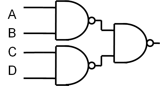
Darstellung eines Minterms durch NAND Funktionen
SOP-Ausdruck (sum of products)
(AB)+(CD)
Verifikation mit einer Wahrheitstabelle
Schaltung zur Realisierung der Normalform
Stellen Sie die Wahrheitstabelle auf.
Geben Sie die logische Gleichung an.
Jedes Gatter hat eine Verz÷gerungszeit von 5 ns.
Geben Sie die maximale Verz÷gerungszeit an.
Schaltung zur Realisierung der Normalform
Stellen Sie die Wahrheitstabelle auf.
Geben Sie die logische Gleichung an.
Jedes Gatter hat eine Verz÷gerungszeit von 5 ns.
Geben Sie die maximale Verz÷gerungszeit an.
Eingõnge
Signale
Ausgõnge
IN2
IN1
IN0
X1
X2
X3
X4
X6
X7
X8
OUT0
OUT1
0
0
0
1
1
1
1
1
1
1
0
0
0
0
1
1
1
0
1
1
1
1
0
0
0
1
0
1
0
1
1
1
0
1
0
1
0
1
1
1
0
0
1
0
1
0
1
1
1
0
0
0
1
1
0
1
1
1
1
0
1
0
1
0
1
0
1
1
1
1
0
0
1
1
0
0
0
1
1
1
1
1
0
0
1
1
1
0
0
0
1
1
1
1
0
0
Geben Sie die logische Gleichung f³r Out0 an:
OUT0 = (IN2 /IN1 /IN3) + (/IN2 IN1 IN0)
Geben Sie die logische Gleichung f³r Out1 an:
OUT1 = (/IN2 IN1/IN0) + (/IN2 IN1 IN0)
Die maximale Verz÷gerungszeit betrõgt 3 * 5 ns = 15 ns.
Ein NAND Gatter hat nur dann eine 0 am Ausgang, wenn alle Eingõnge auf 1 sind.
X4 ist nur dann 0, wenn IN2=1, /IN1=1 und /IN0=1 ist.
Eine õhnliche Schaltung wird im
Versuch 2 realisiert.
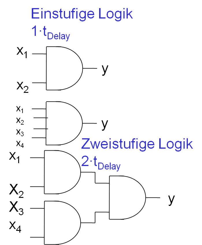
Anzahl Eingõnge, Stufigkeit und Verz÷gerung
Im einfachen Verz÷gerungsmodell gibt es pro Stufe eine Einheitsverz÷gerung
Im einfachen Modell kann man beliebig viele Variablen auf einmal
Verkn³pfen in der praktischen Realisierung ist das nicht m÷glich:
Praktische Realisierungen haben meist bis zu 4 Eingõnge.
Bei mehr Eingõngen verwendet man mehrere Stufen
VHDL Beschreibung
Steuerw÷rter:
Entity, is, port, end, architecture, of, begin, <=, and, end
Trennungszeichen
Strichpunkt ;
Programmierung durch Kopieren und Verõndern.
Struktur
Entity: Schnittstelle: Eingõnge und Ausgõnge
architecture: Verbindung und Funktionen
VHDL Beschreibung
entity und is port (
    X1,X2: in STD_LOGIC;
    Y: out STD_LOGIC);
end und;
architecture logic of und is
begin
    Y <= X1 and X2;
end;
Typ: STD_LOGIC
Wert
Bedeutung
Verwendung
ÆUÆ
Nicht initialisiert
Nicht initialisiertes Signal im Simulator
ÆXÆ
Undefiniert
Mehr als ein Signaltreiber
Æ0Æ
Logische '0'
Boolescher Wert
Æ1Æ
Logische '1'
Boolescher Wert
ÆZÆ
Hochohmig
Tri-State Ausgang
ÆWÆ
Schwach unbekannt
Mehrere Treiber mit L und H
ÆLÆ
Schwache logische '0'
Pull-down Widerstand
ÆHÆ
Schwache logische '1'
Pull-up Widerstand
Æ-Æ,D
Don't care
Logikzustand ohne Bedeutung
Ein Simulator erweitert die Wahrheitstabellen f³r Verkn³pfungen entsprechend.
Ports, Busse und Signale
Eingang und Ausgang einer Schaltung: Port
In: Das Signal kann nur gelesen werden (rechte Seite Signalzuweisung)
Out: Das Signal kann nur gesetzt werden (linke Seite Signalzuweisung)
Buffer: Das Signal kann gelesen und gesetzt werden.
Wertzuweisung: Y <= æ0æ; -- Hochkomma
Bus:
STD_LOGIC_VECTOR, BIT_VECTOR
MY_NIBBLE: in STD_LOGIC_VECTOR(3 downto 0);
MY_NIBBLE <= ō1101ō;
Eine Leitung: Y <= MY_WORD(2);
MY_WORD <= MY_NIBBLE_1 & A & B & C;
Ein Bus wird zusammengesetzt aus einem Bus und mehreren Signalen.
Signal
signal Y1, Y2: STD_LOGIC;
Lokale Leitungen, die gesetzt und gelesen werden k÷nnen.
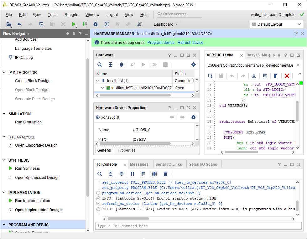
Entwicklungsumgebung (IDE)
Xilinx Vivado
Integrated development environment (IDE).
Entwicklungsumgebungen sehen alle sehr õhnlich aus und sind folgenderma▀en aufgebaut:
Links gibt es den "Flow Navigator" der die Schritte Entwurf("IP Integrator"), Simulation und
Hardware Konfiguration ("RTL Analysis", "Synthesis", "Implementation") bereitstellt.
Entwurf: Zusammenstellung von Schaltungen durch VHDL, Verilog oder vordefinierten Bl÷cken (IP-Catalog).
Simulation: Eine logische Schaltung wird mit geeigneten Stimuli (Eingangssignalen) simuliert.
Mit Hilfe der Simulation erzeugt man eine Wahrheitstabelle um die Schaltung zu verifizieren.
Hardware Konfiguration: Aus einer textuellen Beschreibung soll eine Konfigurationsdatei f³r einen Logikschaltkreis erzeugt werden.
Diese Punkte entsprechen dem Kompilieren und Debuggen einer Programmierumgebung.
In Abhõngigkeit des Schrittes õndern sich die rechts daneben gezeigten Fenster.
Rechts ist der Texteditor mit Syntaxhighlighting.
Schl³sselw÷rter werden farbig hervorgehoben.
In der Mitte ist der Baum mit allen verwendeten Dateien.
Im unteren Bereich sieht man Statusmeldungen (Fehler).
Beispiel: Logikfunktion
entity ANDX is
    Port ( X : in  STD_LOGIC_VECTOR (3 downto 0);
           y : out  STD_LOGIC);
end ANDX;

architecture Behavioral of ANDX is
signal H1:STD_LOGIC;
begin
 h1 <= x(1) and x(2);
 y<= (h1 or x(0)) and x(3);
end Behavioral;
Hier wird das Steuerwort 'signal' verwendet.
Test (1)
ENTITY ANDX_test IS
END ANDX_test;

ARCHITECTURE behavior OF ANDX_test IS
    -- Component Declaration for the Unit Under Test (UUT)
    COMPONENT ANDX
    PORT(
         X : IN  std_logic_vector(3 downto 0);
         y : OUT  std_logic
        );
    END COMPONENT;
   --Inputs
   signal X : std_logic_vector(3 downto 0); -- := (others => '0');
   --Outputs
   signal y : std_logic;
Die entity ANDX_test hat keine Eingõnge oder Ausgõnge.
In der Architecture findet man erst die verwendeten Komponenten (COMPONENT)
und dann die Leitungen oder Register (signal).
Test (2)
BEGIN
	-- Instantiate the Unit Under Test (UUT)
   uut: ANDX PORT MAP (
          X => X,
          y => y
        );
Als erstes wird die zu testende Schaltung (unit under test, uut) implementiert
und verbunden (PORT MAP).
Da die Schaltung ANDX mehrmals verwendet werden kann, wird dieser Instanz
der name uut zugeordnet.
Test (3)
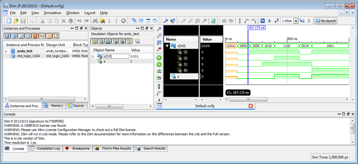
   -- Stimulus process
   stim_proc: process
   begin
 -- hold reset state for 100 ns.
      wait for 100 ns;
 -- insert stimulus here
      x <= (others => '0'); wait for 100 ns;
      x <= "1000"; wait for 100 ns;
      x(1) <='1'; wait for 100 ns;
      x(2) <='1'; wait for 200 ns;
      x(3 downto 2) <= "00"; wait for 100 ns;
      x <= "1001"; wait for 100 ns;
      wait;
   end process;
END;
Mit der Anweisung 'process' kann man eine Abfolge definieren.
Die 'wait' Anweisungen bestimmen das zeitliche Verhalten.
Die Anweisungen werden nacheinander von oben nach unten abgearbeitet.
Nur bei einer expliziten Zuweisung kann sich ein Signal õndern.
Die Entwicklungsumgebung generiert ein Template (leere H³lle) zum Test einer Schaltung.
Man muss nur die zeitliche Abfolge der Signale einf³gen.
Ein Multiplexer in VHDL
Entity
Input
Output
Std_logic
Std_logic_vector
Bus
Architecture
When Anweisung (Statement)
entity Multiplexer_VHDL is
   port   (
      a, b, c, d: in std_logic;
      Sel : in std_logic_vector(1 downto 0);
      Y : out std_logic
   );
end entity Multiplexer_VHDL;

architecture Behavioral of Multiplexer_VHDL is
begin
     Y<= a when Sel="00" else
         b when Sel="01" else
         c when Sel="10" else
         d;
end architecture Behavioral;