7 Segmentanzeige, Schiebeschalter, LED
PMOD Anschlüsse
XADC Analog Digital Wandler
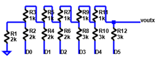
R2R Digital Analog Wandler
Serial interface (COM port) über USB
NodeJS Webserver, HTML User Interface
JavaScript
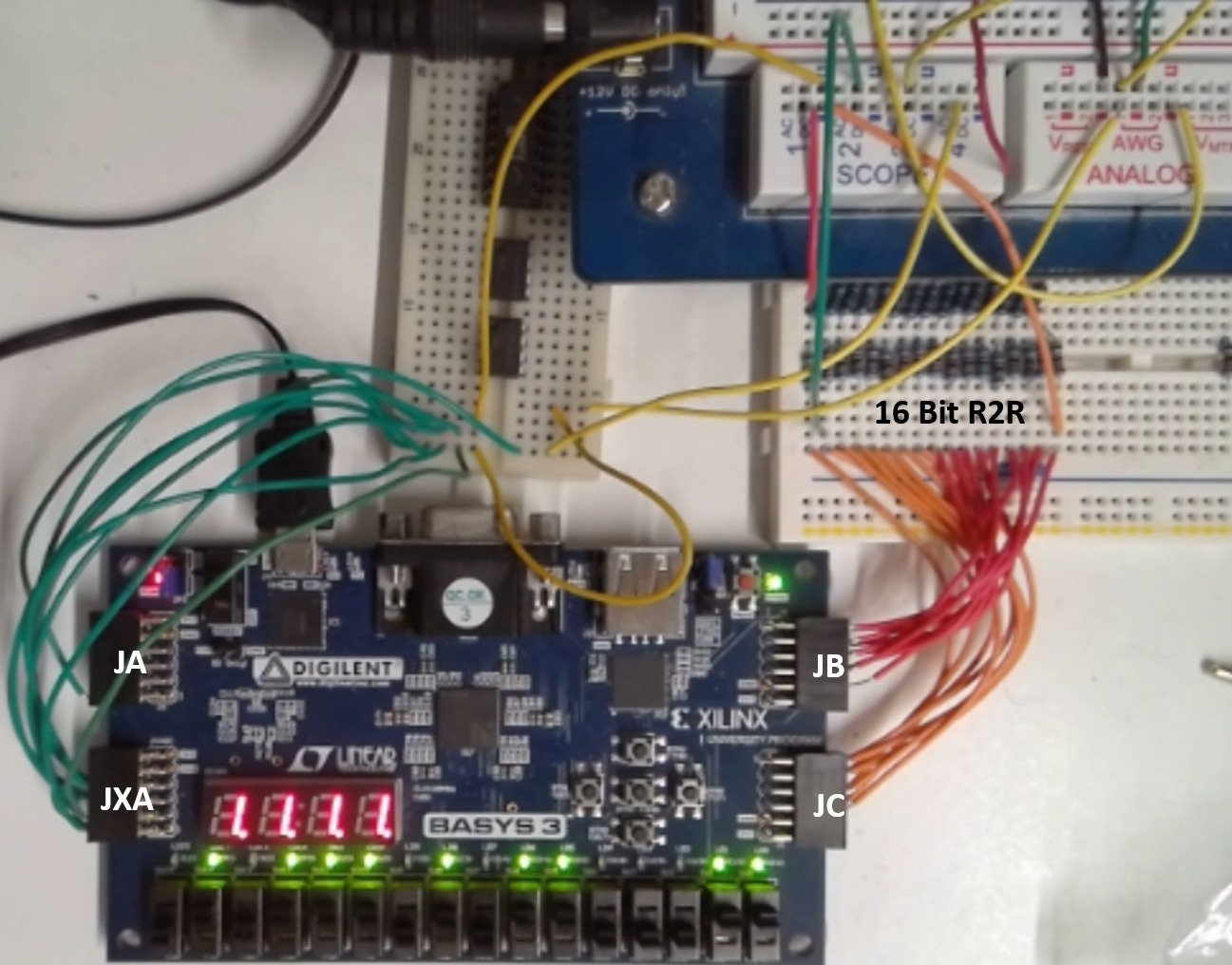
Hier wird ein FPGA board von Digilent für etwa 120.- Euro (2023) als embedded System gezeigt.
FPGAs erlauben es viele taktgenaue Funktionen parallel zu relaisieren, da sehr viele Anschlüsse
zur Verfügung stehen, die einzeln programmiert werden können.
Hier werden die Anschlüsse für 18 Schiebeschalter, 18 LEDs, eine vierstellige 7-Segment Anzeige,
4 PMOD Anschlüsse (mit jeweils 8 programmierbaren Pins), Videoausgang und USB Anschluss verwendet.
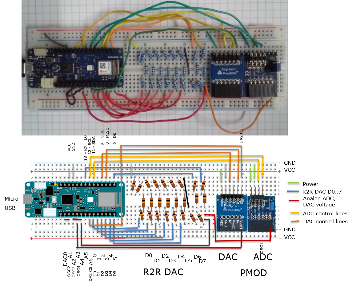
Mikrocontroller Embedded System
Arduino MKR WIFI 1010
1 DAC Digital Analog Wandler
ADC Wandler
Digitale Anschlüsse
SPI, I2C Schnittstellen für externe ADC, DAC
Serial interface (COM port) über USB
NodeJS Webserver, HTML User Interface
JavaScript
Hier wird ein Arduino MKR WIFI 1010 Mikrocontroller Board gezeigt (27.- 2023).
Ausserdem wird ein R2R DAC realisiert, ein DAC DA2 PMOD (20.-) und
ein ADC AD2 PMOD (20.- 2023) sind via SPI und I2C Schnittstelle angeschlossen.
Eine Programmierung in C erlaubt eine schnellere Entwicklung einer Applikation,
die nur Zeitabläufe mit Genauigkeiten im ms Bereich möglich macht.
Digilent:
PMOD AD2 20.-
Analog devices
AD7991 4 channel, I2C, 1us conversion time, 12-bit
Properties of digital signals
Properties:
Resolution
Frequency
Power consumption
Price
Architecture, type
Power supply voltage
Input range
Manufacturing process feature size
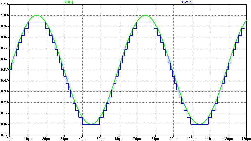
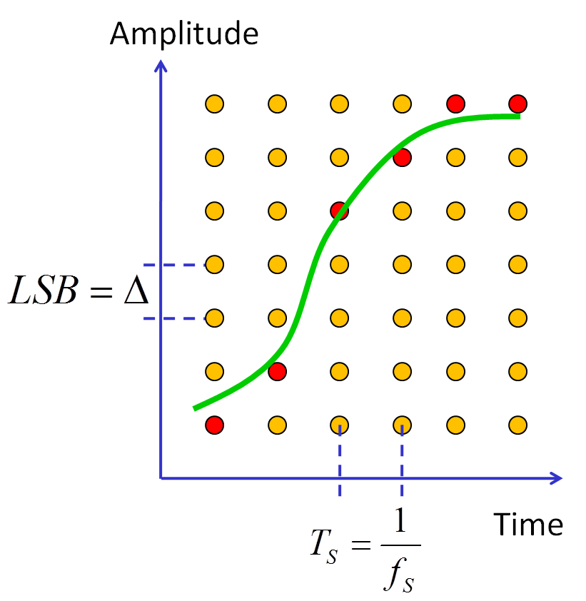
The green analog curve is discretized in time and level resulting in the red points.
The smallest difference in level is called delta Δ or LSB (least significant bit).
The smallest difference in time is called sampling time (ts).
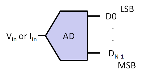
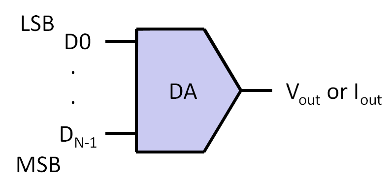
Digital to analog converter metric
Nbit inputs:
digital signals D0..DN-1
for simplicity representing positive binary numbers 0..(2Nbit-1)
D0 is the least significant bit LSB
DNbit-1 is the most significant bit MSB
Analog output signal:
for simplicity voltage
Current and range can be adjusted by additional
analog circuits (amplifier, level shifter).
Metrics:
Nbit: number of Bits
Vref: reference voltage
Vmax=VFS: maximum, full scale voltage
Δ , LSB minimum step size
Es gibt das absolute Least Significant Bit (LSB) und das relative LSB.
\( LSB_{abs} = \frac{Vref}{2^{NBits}} \)
\( LSB_{rel} = \frac{1}{2^{NBits}} \)
Man rechnet einen Spannungswert in einen binären Code um,
den man an den DAC anlegt.
Beispiel: LSBabs = 12 mV, Uout = 1.430 V
Welche Maximalspannung kann ein 10-Bit Wandler mit diesen Daten ausgeben?
Wie gross ist Vref?
Welche Dezimalzahl und Binärcode benötigt der DAC zur Erzeugung von Uout?
Nbit = 10
Vmax = LSB · (2Nbit - 1) = 12 mV * 1023 = 12.276 V
Vref = LSB · 2Nbit = 12 mV * 1023 = 12.288 V
Code = 1.430V / 12 mV = 119.1667
Eine ganze Zahl wird benötigt: 119
Es wird eine Spannung von 119 * LSB = 1.428 V ausgegeben.
The points are the generated measurable values. The straight line only interpolates these values to show a
linear relationship of the values.
DAC sine signal
U(t) = A · sin(ωt)
Erzeuge Codes für positive ganze Zahlen:
\( A = \frac{2^{Nbit} - 1}{2} \)
U(t) = Runde( A · ( 1 + sin(ωt)))
Erzeugung mit festem Zeitraster tCLK
Anzahl Perioden:
1
Anzahl Punkte:
32
NBits:
3
Es wird meist eine Tabelle verwendet, da die Sinusberechnung zu lange dauert.
Je nach Anzahl von Messpunkten und Perioden werden nicht alle möglichen
Ausgangscodes verwendet.
Wenn die Anzahl der Perioden größer ist als die halbe Anzahl der Punkte sieht man Aliasing.
Punkte 16: Periode 1, sieht genauso aus wie Periode 15, 17, 31, 33 ..
Man spricht von Nyquistzonen und undersampling.
Es wird meist eine Tabelle verwendet, da die Sinusberechnung zu lange dauert.
Spezielle Hardware implementiert eine Sinusberechnung mit Reihenentwicklung.
Komplexe Rechnung kann auch verwendet werden.
#define HWORDS 1024       // Buffer length should be 4 * NCODE to excercise all codes
#define NCODE 256        // Number of codes 2^8
volatile uint16_t sintable1[HWORDS];
volatile uint16_t periods;

  for (uint16_t i = 0; i < HWORDS; i++)        // Calculate the sine table with HWORDS entries
  {
    sintable1[i] = (uint16_t)((sinf(2 * PI * (float)i / (float)HWORDS) + 1) / 2 * (NCODE-1) );
  }

  periods = 1;       //   number of periods (odd number) per HWORDS samples

  for (uint16_t i = 0; i < HWORDS; i++)        // Step through sintable array
  {
    Outputvalue = sintable1[ (i * periods) % HWORDS];
  }
Beispiel: DAC
Datenblatt des Mikrocontrollers
Vref=3.3V
Nbit = 10
Berechnen Sie die kleinste Schrittweite.
Mit welcher Genauigkeit muß die Schrittweite angegeben werden?
Welcher Code wird für 2.000 V Ausgangsspannung benötigt.
Wie groß ist die Ausgangsspannung wirklich?
Nbit: Number of Bits
D0..DN-1: Binary weighted data lines
Vin: Positiv input voltage
Vmax: Maximum input voltage
VFS: Full scale voltage
Vref: Reference voltage
Δ = LSB: minimum resolvable input
For small Nbit there is a significant difference LSB or Δ between
Vmax, VFS and Vref.
In general \( V_{max} = V_{FS} = V_{ref} - LSB \) (Baker).
For large Nbit, LSB gets small and Vmax = VFS ≈ Vref.
Ideal analog-to-digital converter
An analog voltage or current is transfered into a digital output.
Input range is positiv.
Uniform, binary digital encoding
AD Transfer Characteristic
Transition depends on measurement accuracy and step size.
Vref = 1V
Nbit = 2
LSB = 0.25V
Upper voltage limit (transition voltage) for a digital output code:
Attention rounding of LSB:
4095 * 976.56 uV = 3.999 V
4095 * 976 uV = 3.996 V
3 mV Difference in calculation versus LSBabs 0.976 mV
Kalibrierung
Man misst bei einer sehr hohen Spannung Vmax den maximalen Code Cmax.
Man misst bei einer sehr niedrigen Spannung Vmin den minimalen Code Cmin.
Man berechnet LSBreal:
Offset and gain error will be fixed during manufacturing.
A trimmable amplifier is used.
In this lecture first the LSB or Δ is calculated from
the first and last points of the transfer curve.
Then the offset is calculated for the first code or first transition voltage.
Then static errors differential non linearity (DNL) and
integral non linearity (INL) are calculated.

 \[ \Delta = LSB = \frac{V_{ref}}{2^{Nbit}} \]
\[ N_{bit} = log_2 \frac{V_{ref}}{\Delta} = ld \frac{V_{ref}}{\Delta} \]
\[ V_{max} = V_{ref}- \Delta \]
\[ \Delta = LSB = \frac{V_{ref}}{2^{Nbit}} \]
\[ N_{bit} = log_2 \frac{V_{ref}}{\Delta} = ld \frac{V_{ref}}{\Delta} \]
\[ V_{max} = V_{ref}- \Delta \]