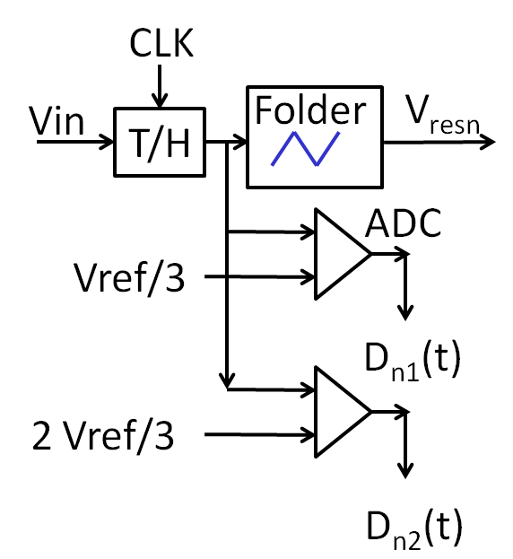
A pipeline ADC
3-bit, one bit per stage, 3-stage folding pipeline ADC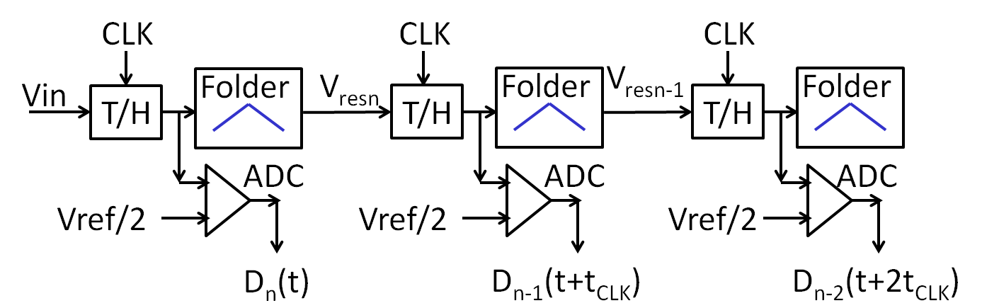
It takes B clock cycles to generate 3 B data bits.
The latency is B · tCLK. Concurrent operation is possible and the sample rate is fCLK.
Properties:
3 stages
Each stage has one sample and hold (T/H), one folder and one 1 bit ADC.
If the output range of the folder is the same as the input range, there is no redundancy or error correction. (1 bit per stage)
Offset and gain error of the folder will cause INL and DNL error and limit performance.
The output range should be a little smaller than the input range to be able to correct folder errors. (0.95 bit per stage)
This circuit needs all sample and hold otherwise the frequency of input voltage at each stage would double causing bandwidth problems.
Since the folding operation does not depend on the ADC high speed operation is possible.
The folder will cause nonlinearities, since the peak of the transfer function will be rounded.
It takes 3 (B) clock cycles to generate 3 (B) data bits.
Since each stage has a separate sample and hold concurrent operation is possible and the sample rate is fCLK.
The latency is B · tCLK.
Variations of the pipeline ADC can have:
- A residue generator instead of the folder requiring a DAC, a subtract stage and a gain stage.
- More than one bit per stage (multiple folding).
Folding pipeline ADC internal voltages
The output code is a Gray code.A typical curve of input voltage, residue voltages and output code is shown below.
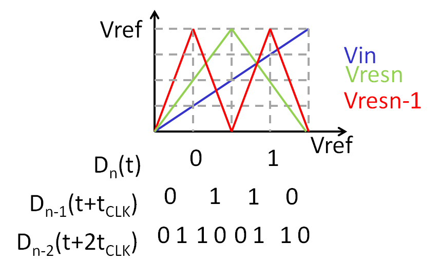
Example pipeline ADC internal voltages
Pipeline ADC with residue generator.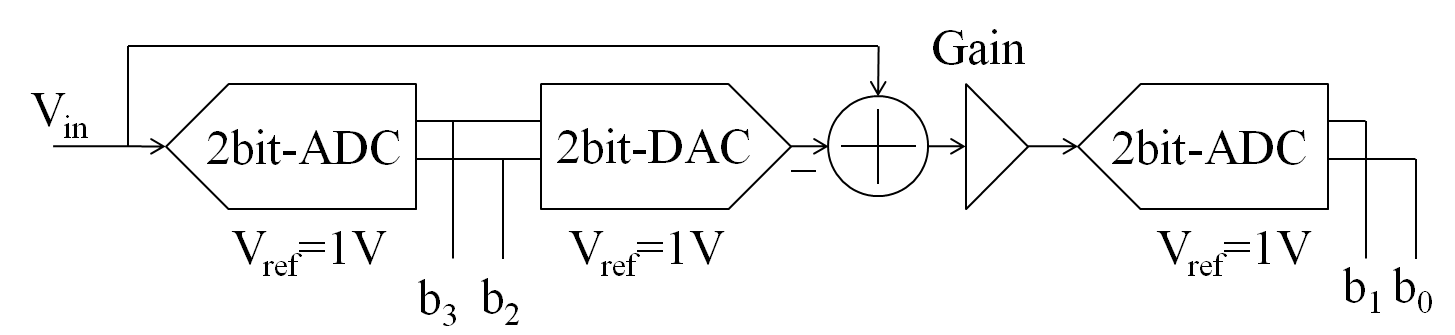
The input ADC has the first transition at 1 LSB instead of normally 1/2 LSB.
Calculate the input range for the b3, b2 codes.
Make a table for the transfer function for a gain of 4 and a gain of 3.
First determine the minimum voltage where b3b2 are changing:
0.25 Vref, 0.5 Vref and 0.75 Vref
For each subrange calculate the residue after the gain stage.
Vres = (Vin - (b3b2)*0.25) * gain
Minimum voltage where b1b0 are changing:
Vres = 0.25 Vref, 0.5 Vref and 0.75 Vref
For each combination b3b2b1b0 Vin can be calculated:
Vin = b3b2 * 0.25 (0.25 * (b1b0) * Vref) / gain
Gain = 4
The second stage sees Vres between 0..1 V at the 2-bit ADC voltage.
b1b0 are also changing at 0.25 Vref, 0.5 Vref and 0.75 Vref
Transfering this to the input means dividing the voltage by the gain:
0.0625 V, 0.125 V, 0.1875 V
Now the table can be filled:
The transfer curve will be limited and cut off at 0V and Vref.
0.25 Vref, 0.5 Vref and 0.75 Vref
For each subrange calculate the residue after the gain stage.
Vres = (Vin - (b3b2)*0.25) * gain
Minimum voltage where b1b0 are changing:
Vres = 0.25 Vref, 0.5 Vref and 0.75 Vref
For each combination b3b2b1b0 Vin can be calculated:
Vin = b3b2 * 0.25 (0.25 * (b1b0) * Vref) / gain
Gain = 4
The second stage sees Vres between 0..1 V at the 2-bit ADC voltage.
b1b0 are also changing at 0.25 Vref, 0.5 Vref and 0.75 Vref
Transfering this to the input means dividing the voltage by the gain:
0.0625 V, 0.125 V, 0.1875 V
Now the table can be filled:
| Code b3b2b1b0 | Nr | Vinmin(Gain=4) [Vref] |
| 0000 | 0 | --- |
| 0001 | 1 | 0 + 0.0625 |
| 0010 | 2 | 0 + 0.125 |
| 0011 | 3 | 0 + 0.1875 |
| 0100 | 4 | 0.25 |
| 0101 | 5 | 0.25 + 0.0625 |
| 0110 | 6 | 0.25 + 0.125 |
| 0111 | 7 | 0.25 + 0.1875 |
| 1000 | 8 | 0.5 |
| 1001 | 9 | 0.5 + 0.0625 |
| 1010 | 10 | 0.5 + 0.125 |
| 1011 | 11 | 0.5 + 0.1875 |
| 1100 | 12 | 0.75 |
| 1101 | 13 | 0.75 + 0.0625 |
| 1110 | 14 | 0.75 + 0.125 |
| 1111 | 15 | 0.75 + 0.1875 |
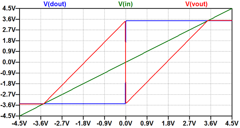
Practical Opamp Realisation with 1 Bit per stage
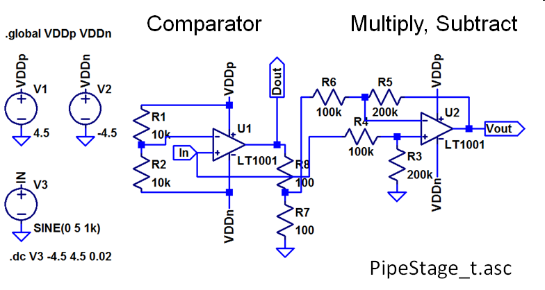
Vout = 2 ( Vin - 0.5 Dout)
On the left the comparator is shown, on the right the folding and amplification stage.
Accuracy is limited by generating the correct level after the comparator and having the right gain at the multiply and add stage. Speed is limited by the critical path from small input difference change of comparator to full level swing of the output to generate residue.
Accuracy is limited by generating the correct level after the comparator and having the right gain at the multiply and add stage. Speed is limited by the critical path from small input difference change of comparator to full level swing of the output to generate residue.
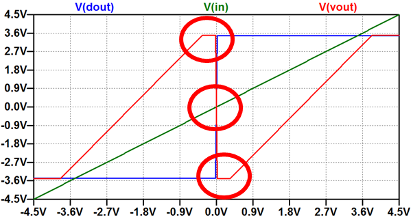
Practical Realisation Simulation Output
|
Comparison of ideal case and gain error. (Picture on the right) Comparison of ideal case and offset error. Discussion: Clipping of output (red circles) limits the resolution of the ADC. (R7=150 Ω) There is a dead zone at the center of the curve. No code change will happen in the dead zone defining and limiting LSB. Reduction of output reduces the input range.(R7=70 Ω) Offset error (RE=1000kΩ) will give missing codes. (Next slide) PipeStage5Bit.asc |
  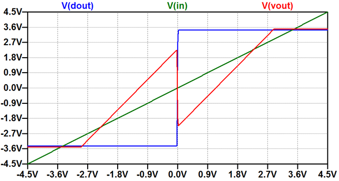 |
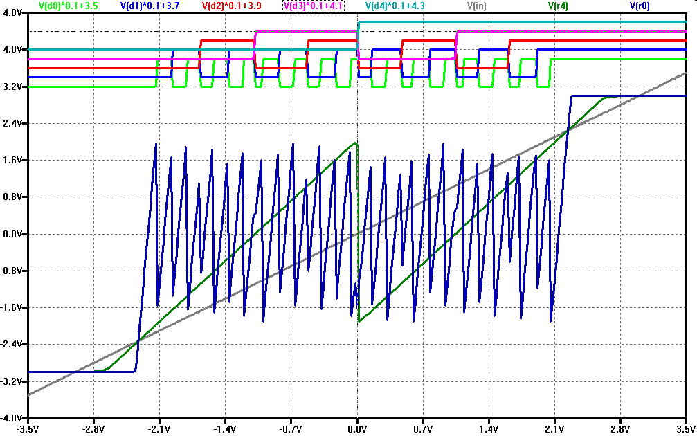
Staying Inside the Box 1
The pink rectangle shows the operation range of the pipeline ADC.
The rectangle is defined by crossing of V(vin) = V(vinx) and Vres (V(voutx)).
For an input voltage close to mid level the code 01111 or 10000 is expected.
Looking at the graph dashed arrows show the operation.
Since the gain of the stage is lower than expected a mid level voltage is not mapped to a maximum Vres (01111) or a minimum Vres (1000).
Following the dashed arrows a code of 01110 is generated.
Code 01111 will not be generated and is missing.
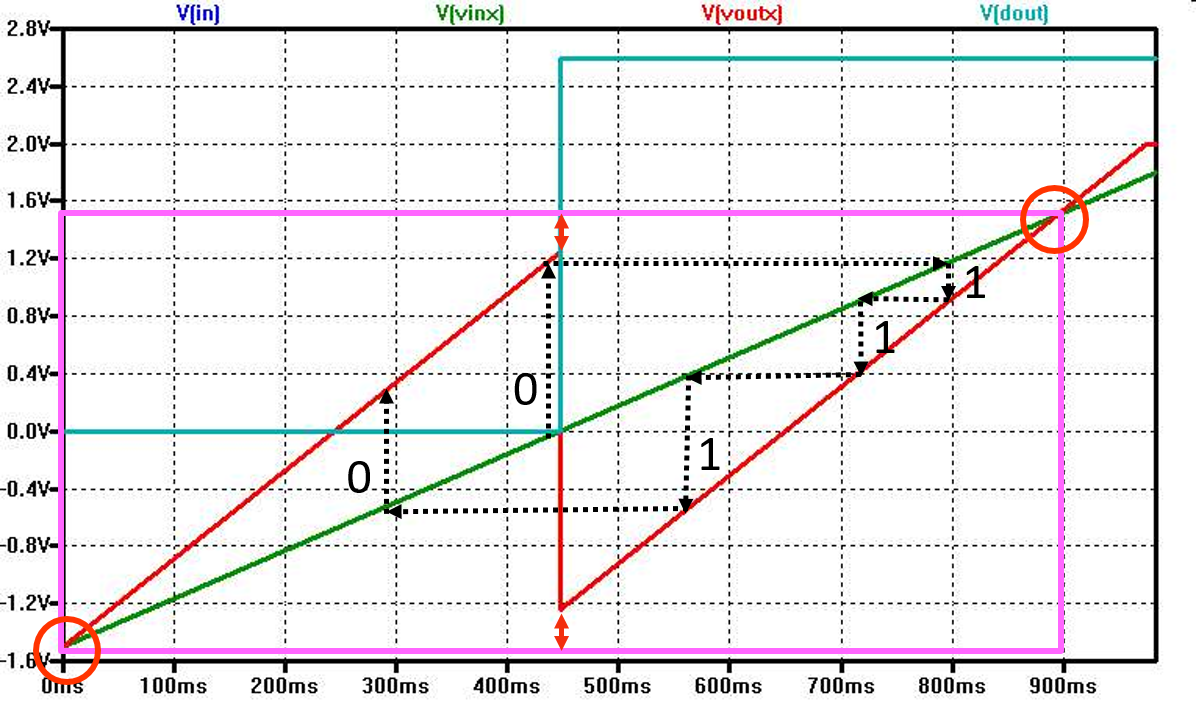
Staying Inside the Box 2
The residue of the 5th stage has varying maxima and minima.
The frequency of the signal at the 5th stage would be 32 times higher than the input ramp frequency.
To limit the maximum frequency sample and holds between stages are used.
Matching of input and output range is very important and difficult.
Simulation and Calibration of a pipeline ADC
|
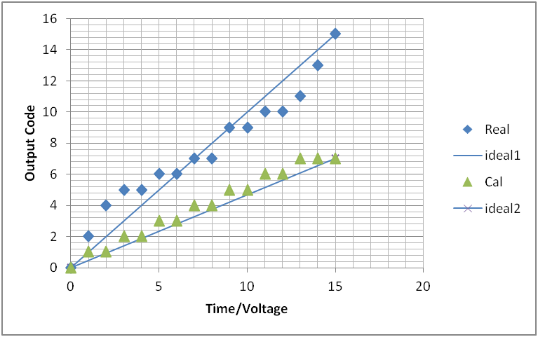
ADC Simulation 4 bit pipeline ADC Gain Error 2.1 Gain Error 1.9 Typical output codes: Missing output codes: gain low and has margin. Changing slope of transfer characteristic: amplifier non linear Calibration: Condense codes and use lowest slope. FFT and ADC Calibration |
 |
Simulation and Calibration of a pipeline ADC
4-bit gain 1.7 nonlinear folding pipeline ADC:
Folding function: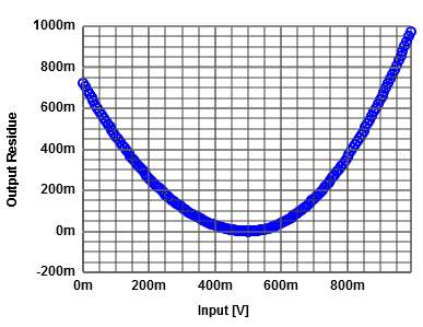
|
Transfer function: |
FFT: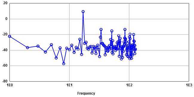
|
|
ENOB: (16.08 dB - 1.76 dB)/6.02 dB = 2.38 Calibration: ENOB: (16.5 dB - 1.76 dB)/6.02 dB = 2.44 |
Calibration: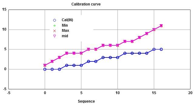
|
FFT: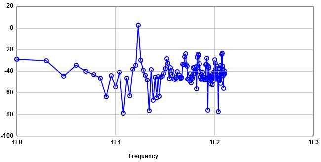
|
Calibration helps to overcome missing codes and non linearities.
Details of simulation:
Signal 9.34 dB Noise -6.73 dB
1st Harmonic -13.56 dB Only noise -15 dB
Calibration:
Signal 2.6 dB Noise -13.9 dB
1st Harmonic -23.62 dB Only noise -20 dB
Gain 1.7 nonlinear folding pipeline ADC:
8-bit: 33.14 dB - 17.09 dB = 16.05 dB
8-bit calibrated: 13.86 dB - (- 12.19 dB) = 26.05 dB
10-bit: 45.45 dB - (29.16 dB) = 16.3 dB
10-bit cal: 13.99 dB - (-13.34 dB) = 27.33 dB
1.58 bit stage for a pipeline ADC
|
There are 3 codes possible: 00,01,11 ld(3) = 1.58 bits |
 |