Interface Electronics12 Sigma Delta Oversampling ADCProf. Dr. Jörg Vollrath11 Pipeline ADC |
Video Lecture: Oversampling Sigma Delta ADC
|
Länge: |
0:0:0 Oversampling ADC 0:4:36 Sigma Delta ADC Architecture 0:12:38 First order passive Sigma Delta Modulator 0:16:51 Internal voltage calculation 0:17:10 0 0:17:10 Example Sigma Delta 0:19:46 Transfer function 0:22:10 f3dB = 15.9 kHz 0:25:46 Output data sequence 0:29:16 dt/R/C = 0.05 0:33:6 Time sequence of voltages 0:36:6 High level simulator (webpage) 0:42:12 LTSPICE simulation sine 0:48:4 General signal and noise transfer function 0:51:14 Noise Shaping 0:52:48 Digital filter and decimator 0:56:16 Example simulation ramp 1:0:46 Example simulation sine 1:5:46 Discussion understanding and simulation 1:9:21 Increasing Signal to noise with oversampling |
Review and Overview
Review:Overview:
- Various ADC architectures
- Data converter systems:
Nyquist rate, oversampling, undersampling - Objectives sigma delta converter
- Oversampling, filter, aliasing, speed and resolution
- History of oversampling
- Sigma Delta converter architecture
- Passive 1st order sigma delta converter: schematic
- Passive 1st order sigma delta converter: SPICE
- Passive 1st order sigma delta converter: signal example
- Passive 1st order sigma delta converter: RC and filter
History
Nyquist ADCOversamplingfCLK = OSR · 2 · fbw Clock frequency is much higher than bandwidth. Pulse count Modulation (PCM)Predictive CodingQuantize difference of the signal Sigma delta converter |
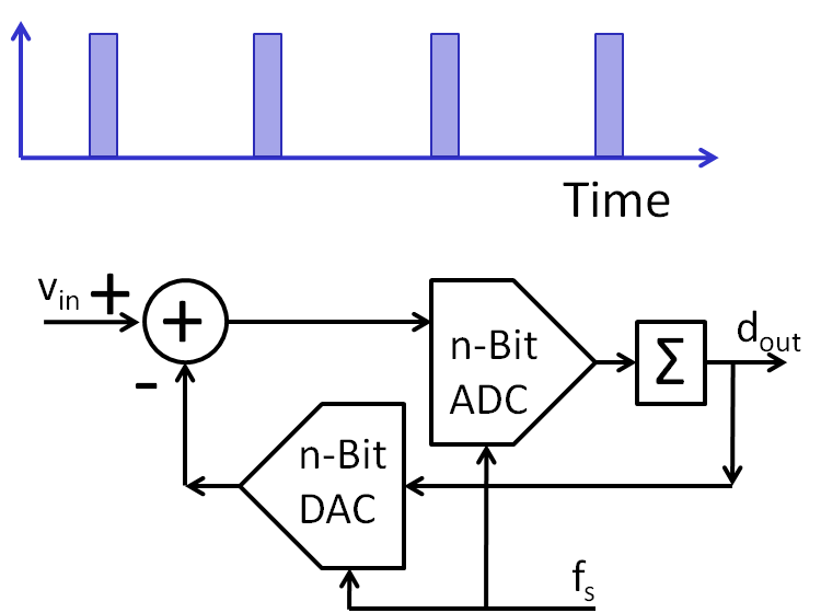 |
Sigma Delta ADC Architectures
 |
   |
Questions
How to build a sigma delta ADC?
- Literature, Theory:
Baker, Razavi, Holberg, Schreier, Wikipedia, SSCC - LTSPICE simulation
- Digital filter
- Need for high level simulation
- Realization, Measurement
- Review, Comparison
Overview
- Internal voltages: LTSPICE, high level simulation
- Transfer function: Stability and noise shaping (SNR)
- Signal to noise ratio and architectures
First order, second order, higher order - Digital filters
Digital time domain circuits and frequency representation
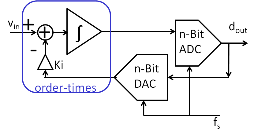
Realization - Example realization
Passive
Active: continous time realization (CT)
Cascaded (MASH)
Active: switched capacitor realization (SC)
CIFB architecture
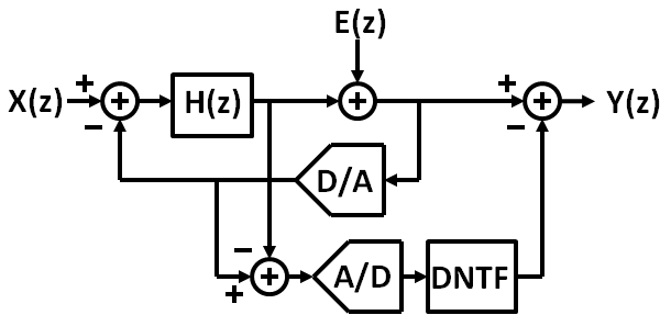
First order passive Sigma Delta Modulator
Internal voltage levels:The voltage V(INT n+1) at clock cycle n+1 is:\( V_{int n+1} = V_{int n} + \frac{\delta t}{C} \left( \frac{ V_{not(Dout)} - V_{int n}}{R} + \frac{V_{in} - V_{int n}}{R} \right) \) \( V_{int n+1} = V_{int n} + \frac{\delta t}{C \cdot R} \left( V_{not(Dout)} + V_{in} - 2 \cdot V_{int n} \right) \) \( \delta t \) is the period of the clock. \( V_{Dout} \) in a real logic circuit is 0V or VDD. \( \frac{\delta t}{C \cdot R} = \frac{2 \pi f_{sample}}{f_{CLK}} = \frac{2 \pi }{OSR} \) These equations are used for a high level simulation. High level simulation: 1st order sigma delta simulation Since Vint has to stay between 0V and VDD: \( \frac{\delta t}{C \cdot R} 2 V_{DD} \lt V_{DD} \) \( C \cdot R \gt \frac{2}{f_{sample} } \) \( \frac{1}{C \cdot R} \lt \frac{f_{sample} }{2} \) The bandwidth limit of RC has to be smaller than fsample/2. The bandwidth limit of RC has to be greater than the interested bandwith. fsample/2/OSR \( 2 \pi f_{bw} \lt \frac{1}{C \cdot R} \lt \frac{f_{sample} }{2} \) |
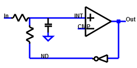
On the left the difference of V(in) and V(D) is integrated and then
compared with V(CMP). The comparator operates with the clock frequency and
gives for each clock cycle a new value.
A simple passive first order sigma delta converter uses resistors and capacitances.
This circuit is according to Baker, "CMOS integrated cicuits", Figure 6.4
A simple passive first order sigma delta converter uses resistors and capacitances.
This circuit is according to Baker, "CMOS integrated cicuits", Figure 6.4
Example: First order passive Sigma Delta Modulator
The circuit with R = 1 kΩ, C= 20 nF is operated with VDD = 1 V, VCMP = 0.5 V and fS = 1 MHz.What is the maximum allowed input voltage?
What is the cut-off frequency of the RC input low pass?
Calculate vout(t) for 4µs if vin=0.3V. The starting value for vint=VCM and vout=0V. Assume a constant current through R for a sampling cycle.
| t [µs] | 0 | 1 | 2 | 3 | 4 |
| vin | 0.3V | ||||
| vint | 0.5V | ||||
| vout | 0V |
| t [µs] | 0 | 1 | 2 | 3 | 4 |
| vin | 0.3V | 0.3V | 0.3V | 0.3V | 0.3V |
| vint | 0.5V | 0.515V | 0.479V | 0.496V | 0.511V |
| vout | 0V | 1V | 0V | 0V | 1V |
\( \frac{\delta t}{R C} = 0.05 \)
Verification with simulation: 1st order sigma delta simulation
1st order passive Sigma Delta high level simulation
High level simulation: 1st order sigma delta simulation
- Internal voltage simulation: Verification of result from previous calculation
- Ramp test: Dead zones and noisy transition
- Digital filter realisation: Averaging, SINC, droop, bitwidth
- FFT: Signal to noise improvement with OSR and filter
General signal and noise transfer function
A first order sigma delta analog digital converter.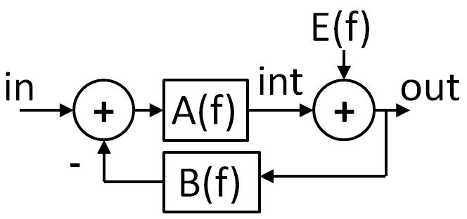
\( V_{out}(f) = V_{in}(f) \frac{A(f)}{1 + B(f) A(f)} + E(f) \frac{1}{1 + B(f) A(f)} \)
\( V_{out}(f) = V_{in}(f) \frac{1}{B(f) + \frac{1}{A(f)}} + E(f) \frac{1}{1 + B(f) A(f)} \)
There is a signal transfer function and a noise transfer function.
\( V_{out}(f) = \left( V_{in}(f) - B(f) V_{out}(f) \right) A(f) + E(f) \)
\( V_{out}(f) = V_{in}(f) A(f) - B(f) V_{out}(f) A(f) + E(f) \)
\( V_{out}(f) \left( 1 + B(f) A(f) \right) = V_{in}(f) A(f) + E(f) \)
\( V_{out}(f) = V_{in}(f) \frac{A(f)}{1 + B(f) A(f)} + E(f) \frac{1}{1 + B(f) A(f)} \)
Signal transfer function (STF):
\( STF(f) = \frac{A(f)}{1 + B(f) A(f)} \)
Noise transfer function (NTF):
\( NTF(f) = \frac{1}{1 + B(f) A(f)} \)
First order passive Sigma Delta Modulator signal and noise transfer function
\( \frac{v_{in} - v_{int}}{R} + \frac{-v_{out} - v_{int}}{R} = i_{int} \)
\( v_{in} - v_{int} - v_{out} - v_{int} = i_{int} R \)
\( v_{in} - v_{out} - 2 \cdot v_{int} = i_{int} R \)
\( v_{in} - v_{out} = i_{int} R + 2 \cdot v_{int}\)
\( i_{int} = v_{int} j \omega C \)
\( v_{int} = \frac{v_{in}-v_{out}}{j \omega C R + 2} \)
vint = A(f) · (vin - B(f) vout)
\( B(f) = 1 \) \( A(f) = \frac{1}{j \omega C R + 2} \)
\( V_{out}(f) = \frac{V_{in}}{C R} \frac{1}{j \omega + \frac{3}{R C}} + E(f) \frac{j \omega + \frac{2}{R C}}{j \omega + \frac{3}{R C}} \)
Comparing the equation for the internal voltage vint with the general signal
and noise transfer function gives:
\( V_{int}(f) = A(f) \cdot ( V_{in} - V_{out} \cdot B(f) ) \)
\( B(f) = 1 \)
\( A(f) = \frac{1}{j \omega C R + 2} \)
\( V_{out}(f) = V_{in} \frac{1}{j \omega C R + 3} + E(f) \frac{j \omega C R + 2}{j \omega C R + 3} \)
\( V_{out}(f) = \frac{V_{in}}{C R} \frac{1}{j \omega + \frac{3}{R C}} + E(f) \frac{j \omega + \frac{2}{R C}}{j \omega + \frac{3}{R C}} \)
Noise shaping
|
Signal pole: ω=3/(RC) Noise zero: ω=2/(RC) Noise pole: ω=3/(RC) Position fclk Position fbw = 3/(2 π R C) Noise is digitally filtered. \( \epsilon_q = \frac{LSB}{\sqrt{12}} \) \( - 20 log \sqrt{12} = -10.8 dB \) |
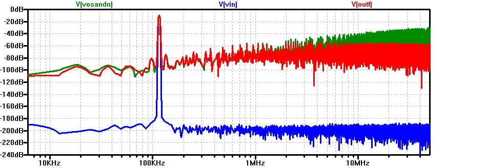
FFT and Noise shaping
Circuit: SigmaDeltaRC.asc
tCLK = 200ns; fCLK = 5 MHZ
16k points makes 3.2768 ms transient simulation plus initialization.
fx = 1/2/pi/R/C=1/2/pi/100k/10p Hz = 160 kHz
OSR = 9.9
dSNR = 30 log(OSR) = 30 dB
ENOB = 30 dB / 6 dB = 6 Bit
Simulation time: 20 min
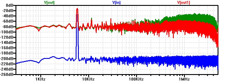
Figure: SigmaDeltaRC_Sig200k10p32k.jpg
tCLK = 200ns; fCLK = 5 MHZ
16k points makes 3.2768 ms transient simulation plus initialization.
fx = 1/2/pi/R/C=1/2/pi/100k/10p Hz = 160 kHz
OSR = 9.9
dSNR = 30 log(OSR) = 30 dB
ENOB = 30 dB / 6 dB = 6 Bit
Simulation time: 20 min
Figure: SigmaDeltaRC_Sig200k10p32k.jpg
SigmaDeltaRC_FFT200k10p32k.jpg
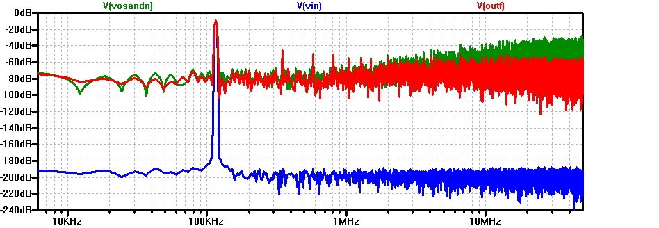
Change C=100pF; OSR = 100;
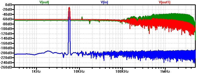
Figure: SigmaDeltaRC_FFT200k100p32k.jpg
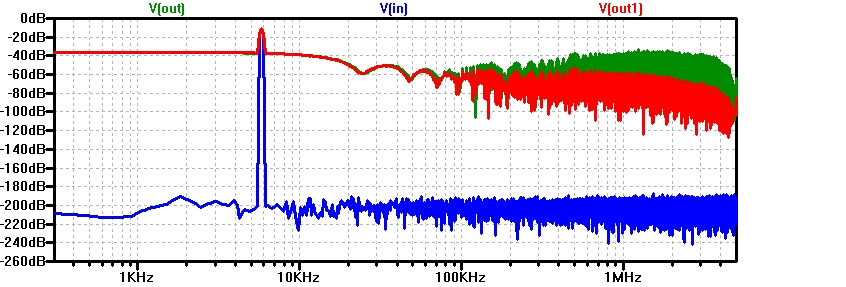
Figure: SigmaDeltaRC_FFT200k1000p32k.jpg
Ideal sample hold comparator and inverter give more signal noise ratio.
SPICE/Passive_1st_SigmaDelta/__SigmaPassiveRC.asc
SigmaDeltaRCB_FFT10k20p16k.jpg
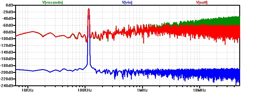
SigmaDeltaRCB_FFT10k200p16k.jpg
SigmaDeltaRCB_FFT10k2000p16k.jpg
SigmaDeltaRCB_FFT10k20000p16k.jpg
Change C=100pF; OSR = 100;
Figure: SigmaDeltaRC_FFT200k100p32k.jpg
Figure: SigmaDeltaRC_FFT200k1000p32k.jpg
Ideal sample hold comparator and inverter give more signal noise ratio.
SPICE/Passive_1st_SigmaDelta/__SigmaPassiveRC.asc
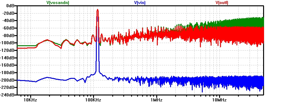
SigmaDeltaRCB_FFT10k20p16k.jpg
SigmaDeltaRCB_FFT10k200p16k.jpg
SigmaDeltaRCB_FFT10k2000p16k.jpg
SigmaDeltaRCB_FFT10k20000p16k.jpg
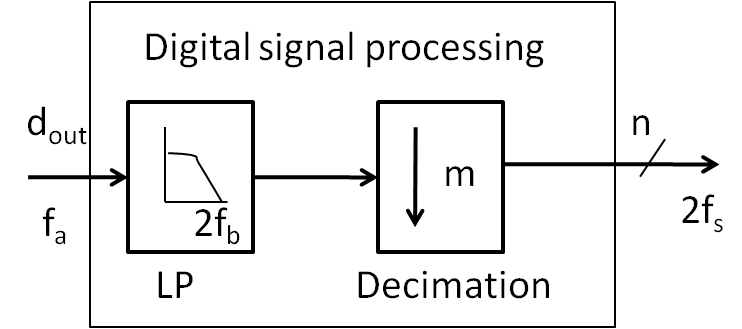
Digital filter and decimator
|
SINC Filter Filter order: SINC, SINC2, SINC3 The order of the filter has to be one more than the sigma delta modulator to realize the full signal to noise benefit. |
A decimating Sinc2 filter has the following schematic with 2 integrators and 2 differentiators: 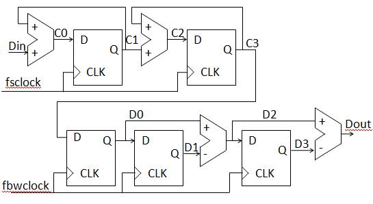 |
How to physically realize the filter?
Width of the registers?
Width of the registers?
Calculating Signal to noise ratio
\( V_{noise,RMS}^{2} = 2 \int_0^{BW}{|NTF(f)|^2|V_{Qe}(f)|^2} df \)
Quantization noise spectral density divides the quantization error with sampling frequency:
\( |V_{Qe}(f)|^2 = \frac{V_{LSB}^{2}}{12 f_{sample}} \)
Transfer function:
\( V_{out}(f) = STF(f) v_{in} + NTF(f) V_{Qe}\)
First order passive modulator :
\( V_{out}(f) = \frac{V_{in}}{C R} \frac{1}{j \omega + \frac{3}{R C}} + \frac{E(f)}{R C} \frac{j \omega R C + 2}{j \omega + \frac{3}{R C}} \)
Since signal transfer function and noise transfer function have the part:
\( STF(f) = \frac{1}{j \omega + \frac{3}{RC}} \)
This cancels out for signal to noise ratio.
Calculating Signal to noise ratio (continued)
\( V_{noise,RMS}^{2} = 2 \frac{V_{LSB}^{2}}{12 f_{sample}} \int_0^{BW}{(2 \pi f R C + 2)^2} df \)
\( V_{noise,RMS}^{2} = 2 \frac{V_{LSB}^{2}}{12 f_{sample}} \left( {(2 \pi R C )^2} \frac{BW^3}{3} + 4 \pi R C \frac{BW^2}{2} + 4 BW \right) \)
Sinc-shaped lowpass filter:
\( BW = \frac{f_{sample}}{2 OSR} \)
First part only: \( V_{noise,RMS}^{2} = \frac{V_{LSB}^{2}}{12 } {(2 \pi R C)^2} \frac{f_{sample}^2}{12 OSR^{3}} \)
\( SNR = 20 log\frac{V_{signal,rms}}{V_{noise, rms}} \)
\( SNR = 6.02 N + 1.76 - 20 log \frac{(2 \pi R C) f_{sample}}{\sqrt{12}} + 20 log OSR^{\frac{3}{2}} \)
\( SNR = 6.02 N + 1.76 - 20 log \frac{(2 \pi R C) f_{sample}}{\sqrt{12}} + 30 log OSR \)
With no oversampling signal to noise ratio decreases by:
\( d SNR = - 20 log \frac{(2 \pi R C ) f_{sample}}{\sqrt{12}} \)
The maximum value for fRC = 1 / (2 π R C) = 0.5 f sample
. \( d SNR = -20 log(\frac{2}{\sqrt{12}}) = 4.77 dB \) With larger oversampling rates signal to noise ratio improves by 30 log 2 = 9 dB, 9 dB / 6 dB = 1.5 bits for doubling OSR.
Increasing signal to noise with oversampling
|
Graph increasing signal to noise with oversampling
|
Example: fbw = 1 kHz 1. Order 1-bit sigma delta 8-bit resolution desired. |
Signal to noise, FFT, transfer characteristic and oversampling
|
Example: 8-bit signal with 4-bit noise amplitude. Signal: \( V_{rms} = \frac{V_{amplitude}}{\sqrt{2}} \) Noise: Vrms = VPP/6 = Vamplitude/3
|
Passive First Order Sigma dDelta Design
Given: fbw = 10 kHz, fCLK = 1 MHz, VDD = 1 V
\( OSR = \frac{f_{CLK}}{2 \cdot f_{bw}} = 50 \)
\( N_{Bit} = \frac{30 log(OSR) - 5.2}{6.02} = 8 \)
Capacitance is determined by thermal noise:
\( C (T = 300K) = 12 \cdot k_B \cdot T \frac{2^{2 B}}{V_{FS}^{2}} = 3 fF\)
kB: Boltzmann constant (1.38 · 10 -23 m2kg s-2K-1)
T: absolute temperature in Kelvin
B: number of Bits
VFS = VDD: Full scale voltage
Resistance is determined by oversampling rate:
\( \frac{\pi}{OSR} = \frac{1}{f_{CLK} R C}\)
\( R \lt \frac{OSR}{\pi C f_{CLK}} = 16 G \Omega \)
Reasonable C and R values for a discrete realization would be.
C = 0.3 nF, R = 160 k Ω
\( \frac{\delta t}{R C} = \frac{1}{f_{CLK} R C} = 0.0208 \)
Comparator needs high gain and low offset for low maximum input voltage swing:
\( d v_{intmax} = V_{FS} \frac{\delta t}{ C \cdot R} = V_{FS} \frac{2 \pi}{OSR} = 0.12 V \)
\( d v_{intmin} = \frac{V_{FS}}{2^{NBit}} \frac{\delta t}{ C \cdot R} = 0.5 mV \)
High level simulation with these values
dt/R/C = 0.0208
gives:
dvint 20 mV (??)
Sinc2, OSR = 64, DNLmax = 7/20 = 0.35
NFFT = 16k
Signal Periods: 3
1 Bit: Signal: -12 dB, Noise -12 dB
SINC2: Signal -12.04 dB, Noise -59.38 dB, SNR = 47.34, ENOB = 7.57
Signal Periods: 5983, SNR 44.43 dB
OSR = 512 = 8 * 64
SINC2: Signal -12.04 dB, Noise -82.19 dB, SNR = 70.15, ENOB = 11.36
Expected change in SNR = 30 log(8) = 27 dB versus real change of 23 dB
dt/R/C = 0.00208
Same result.
Reference: CMOS Analog Circuit Design, Allen, Holberg
Chapter 10.9: Oversampling Converters
- [56] Single loop 7th order 118 dB (19 dB)
- [54] Single loop 5th order 20 bit:
Thomsen, Bemades, "A digitally Corrrected 20-bit Delta Sigma Modulator", ISSCC, 194-195, Feb 1994 - [60-64] 3rd order: 2-1 MASH
Longo, Copeland, "A 13-bit ISDN-Band Oversampled ADC..", CICC, pp.21.2.1-21.2.4, Jan 1988
Williams, Wooley, "A Third order Sigma-Delta..", JSSC, Vol 29. No. 3, pp.193-202,Mar 1994
Yin, Stubbe, Sansen, "Av16-bit 320 kHz CMOS ADC..", JSSC, Vol. 28, No.6, pp.640-647, June 1993
Rabii, Wooley, " A 1.8-V 0.8um CMOS ADC", JSSC, Vol 32., No. 6, pp.783-796, June 1993
Brandt, Wooley, "50MHz 12b 2MHz ADC", JSSC,Vol. 26, No. 6, pp. 1746-1756, Dec 1991
- [65-67] 4th order: 2-2 MASH
Tenhunen, "An oversampled ..", ISCAS, pp. 3279-3282, May 1990
Ritoniemi et. al., "A Stereo Audio..", JSSC, Vol. 29, No. 12, pp. 1514-1523, Dec 1994
Fujimori et al., "A 5-V 111dB dynamic range", JSSC, Vol. 32, No. 3, pp.329-336, Mar 1997 - [70] 6th order: 2-2-2 MASH
Dedic, " A sixth order", ISSCC Dig. Tech. Papers, pp. 188-189, Feb 1994 - [30] MASH Decimator: Candy,Temes, oversampling Delta-Sigma Data Converters. IEEE Press
- INF4420 Projects in analog/mixed signal CMOS design
Practical realization of a 1st order Sigma Delta converter
Real 1st order passive sigma delta modulator
Hardware: Digilent NEXYS 3 board with Xilinx FPGA tCLK = 100MHz.
Objectives and Challenges
Generate high resolution sine signal
Analysis of different R, C components, oversampling and timing
Data transfer and processing
Hochschule für angewandte Wissenschaften Kempten, Jörg Vollrath, Bahnhofstraße 61 · 87435 Kempten
Tel. 0831/25 23-0 · Fax 0831/25 23-104 · E-Mail: joerg.vollrath(at)fh-kempten.de
Impressum