ADC DAC Ramp Test
|
The ramp test is done by using a pulse signal, which rise time is equal to the complete simulation time. Hence, only the rising ramp from 0 V to 1 V is taken into account. All the simulated values of the output voltage are saved within a .raw file. This .raw file is analysed by using the given function "Read Raw File". The picture underneath is showing the rising ramp and the corresponding output of the ADC DAC setup. 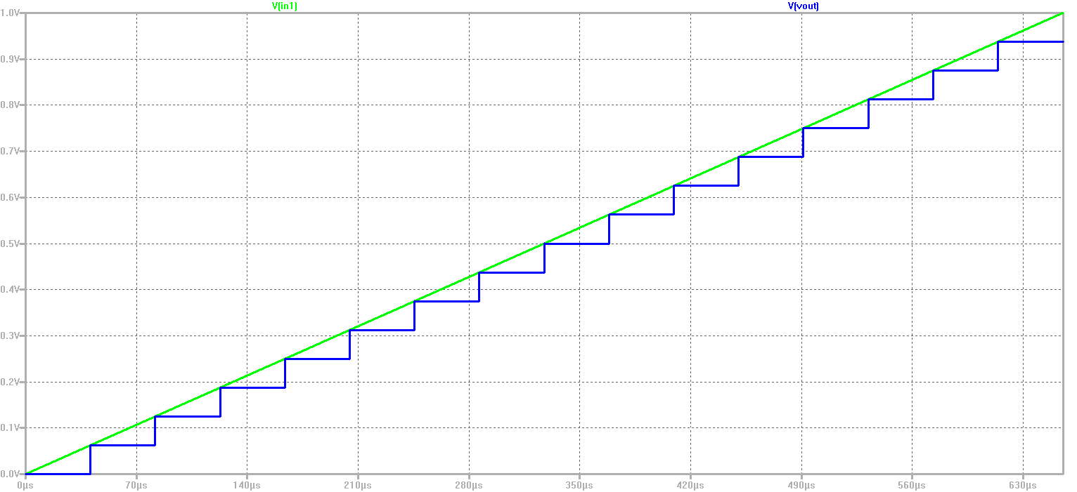 No error in the voltage level can be seen. This is because an ideal ADC and DAC was simulated. |
Analysis of the Ramp Test
|
A 4 Bit ADC DAC test setup was simulated using a ramp input signal. This picture is showing the extracted values and the figure "map to integer". 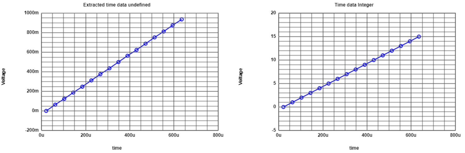 Due to the fact, that the devices are ideal, the INL and DNL is equal to zero for the complete simulation time. The extracted values can be seen in the picture underneath. To draw these graphs, the function "Read Raw File" was used. 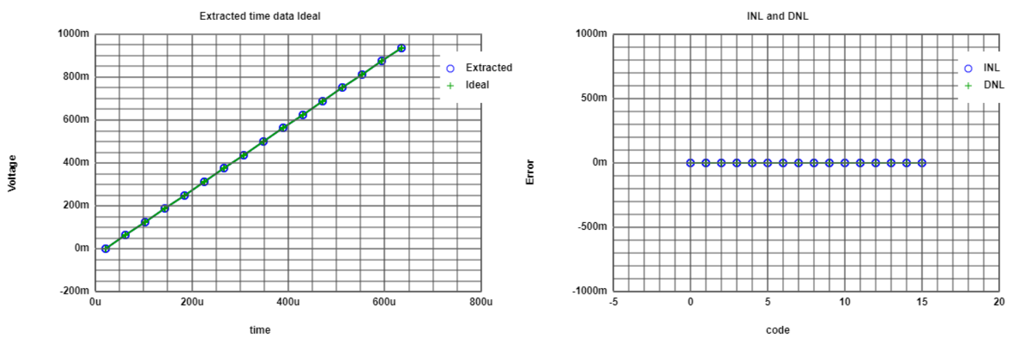 The former two analyses were done by using a time step of 40.96 µs. Corresponding to that time step width, every value of the output voltage is examined once. The maximum output voltage is equal to 937.5 mV, the minimum output voltage to 0 V. By using the number of bits, the LSB can be calculated: LSB = (Vout,max - Vout,min)/((2^n)-1) = (937.5 mV - 0 mV)/((2^4) - 1) = 62.5 mV Every voltage step is met perfectly because of the ideal properties of the used components. Now, a histogramm test is being done. Therefore the time step width is reduced to 5.12 µs. Thus, every voltage step is examined several times. This picture is showing the generated histogram. Each value occurs as often as every other value. 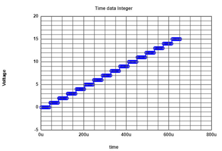 |
ADC DAC Sine Test
|
Now the same schematic is stimulated with a sine signal. The resulting values are again saved within a .raw file. In the picture below the input and the output voltage can be seen. 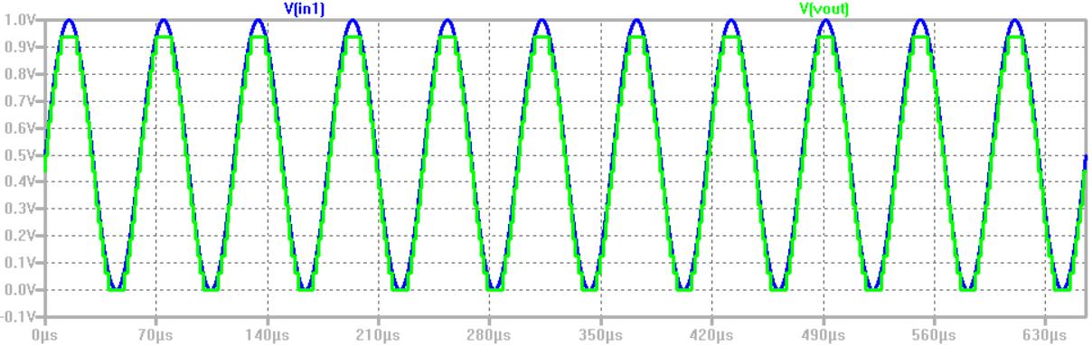 |
Analysis of the Sine Test
|
The same 4 Bit ADC DAC test setup as before was simulated, this time using a sinusoidal input voltage. For the analysis concerning the sine input, the time step width 5.12 µs was chosen. This picture is showing the extracted values and the figure "map to integer". 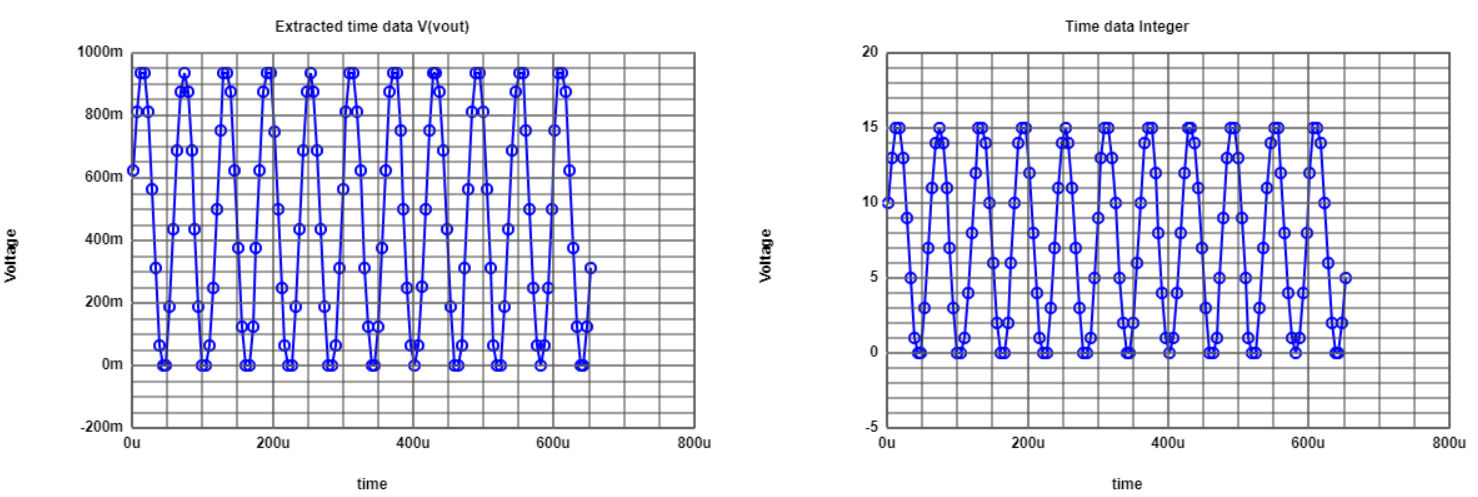 For this simulation, the INL and DNL isn't equal to zero for all the values. The calculated INL and DNL values can be seen in the picture underneath, they are showing the typical shape for a sinusoidal input waveform. For the calculation of the values, the function "Read Raw File" was used. 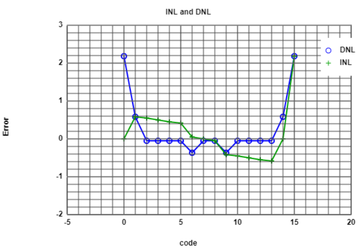 Unfortunately the former calculation of the INL and DNL was based on average values. A more precise calculation will be done now, by the FFT analysis tool. 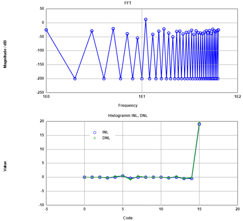 In the upper picture the FFT, the INL and the DNL of the output voltage is shown. During the simulation 11 periods of the signal were simulated. This is causing a peak for the FFT at the frequency 11. These calculations for the INL and DNL are based on a real signal, not on average values. Due to the limited number of frequency points for FFT a lot of frequencies are missing. Due to a computation issue, the INL and DNL waveforms aren't shaped in the typical way. The last picture for this slide is showing a table of magnitudes of the signal and the noise in dB. To calculate the SNR, this equation can be used: SNR = magnitude signal in dB - magnitude noise in dB For instance the SNR of the first listed frequency is equal to 25.8 dB. 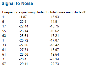 |
Real R2R Circuit - Sine Test
|
The last step of this lab training is to examine a ADC DAC circuit, which contains a real R2R DAC device. An ideal R2R circuit was downloaded from the interface electronics webpage. To receive a real, and not a ideal DAC, some resistances are changed, like it was done in the instruction video. At first the circuit was stimulated with a sine signal. The output voltage can be seen in the picture below. Already at the first glance, it can be seen, that not all the voltage steps have the same size. The biggest deviation from the nominal step width can be seen at the central step around 0.5 V. This is caused by the non-ideal resistance of 1.5 kOhm of the resistor R9. 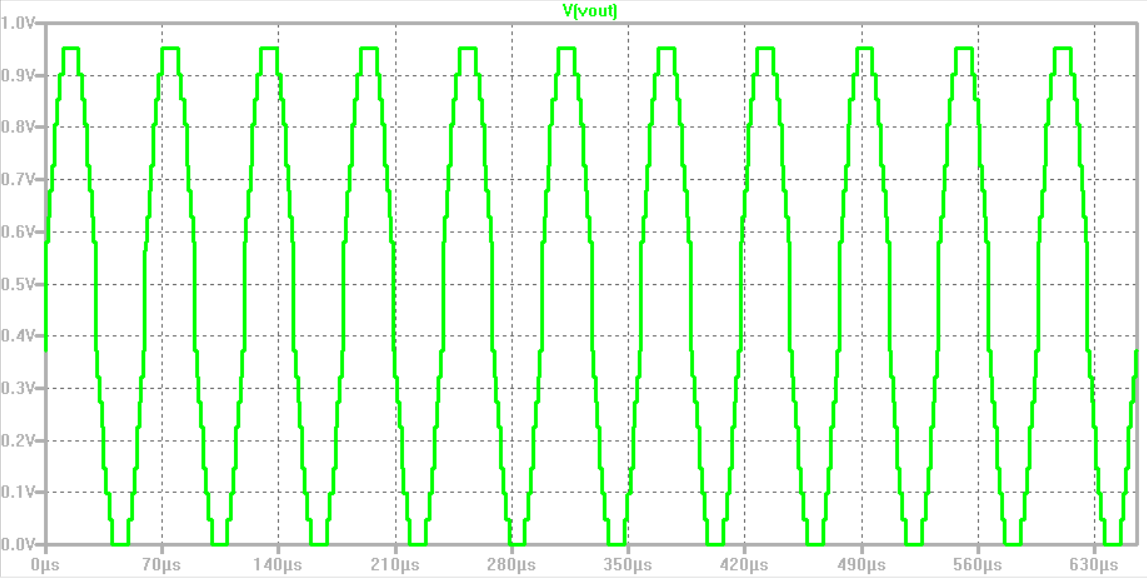 The next picture shows the INL and the DNL error of the simulated circuit. Again the not-typcial curve with the "highflyer" for the last value is resulting. This "highflyer" is caused by a computation issue within the function "FFT Analysis". 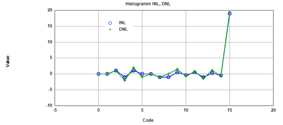 The FFT of the output voltage shows the typical shape. During the simulation 11 periods of the sine signal were processed. This is why the FFT has a peak at the frequency 11. 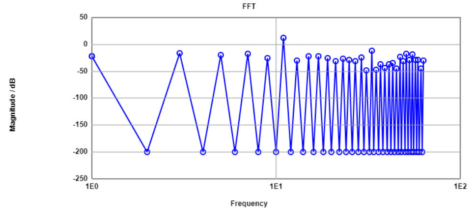 The signal to noise ratio for the signal frequency 11 is equal to 19.17 dB. This is a quite good signal to noise ratio. 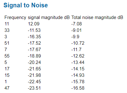 |
Real R2R Circuit - Ramp Test
|
The same circuit as it was used before is no stimulated by a ramp signal. The corresponding output voltage is shown by the picture underneath. Similar to the former simulation, again a big voltage jump around 0.5 V can be seen. Furthermore there are big voltage steps around 0.2 V and 0.75 V. Responsible for these jumps is the non-ideal restistance value of R6. 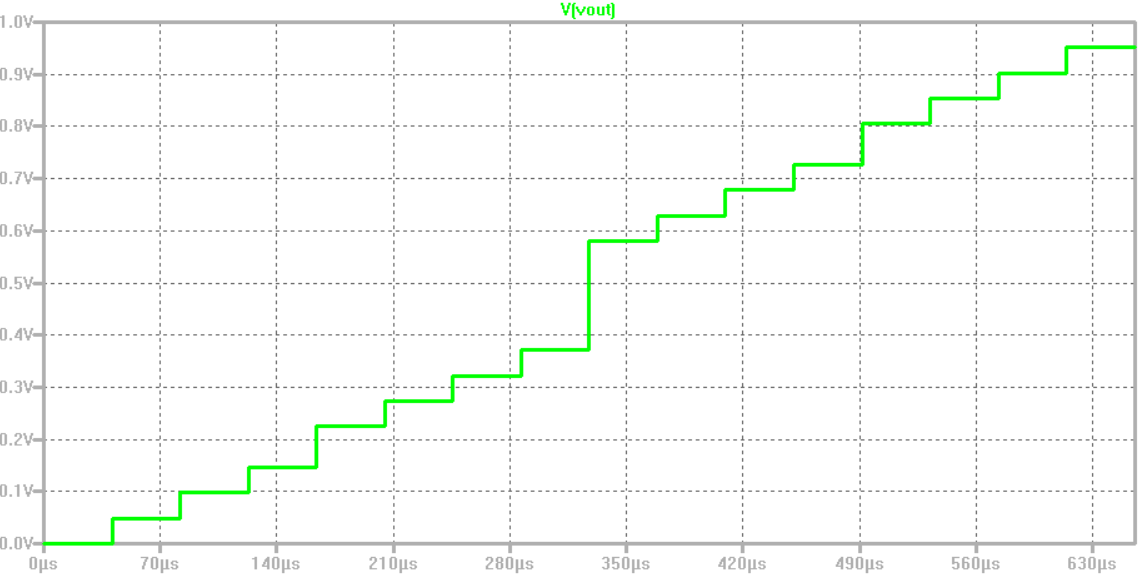 The next picture shows all the extracted values and the INL and DNL error for a time step of 40.96 µs. Located at a voltage of about 0.5 V, the big jump of the output voltage can be seen. Also the INL and DNL error are indicating the non-perfect error curves. Especially the DNL error shows a very striking shaped curve. The big voltage jump around 0.5 V can be seen in the center of the picture at code 8. The smaller deviations around 0.2 V and 0.75 V, which were already mentioned, can also be seen in this curve, this time at the codes 4 and 12. 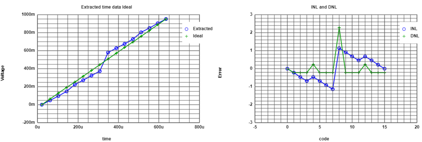 |