Interface ElectronicsLaboratory 03GroupD01, ***03, ARLADC DAC analysis instructions |
Overview
- ADC DAC setup
- Ramp signal: Simulation and analysis of DNL, INL and LSB
- Sine signal: Simulation and analysis of FFT, DNL, INL and LSB
- Summary
- References
ADC DAC steup
|
Here you can see the LTSpice Model of the Simulation. At first the ideal ADC is is simulated with V1, a ramp signal, then with V2, a sine signal. Afterwards the DAC is simulated with the R2R DAC The resistances R6 and R9 are manipulated in order to get a non-ideal DAC. With this non-ideal DAC the INL, DNL and the FFT of the sine signal can be calculated. |
Ramp signal
|
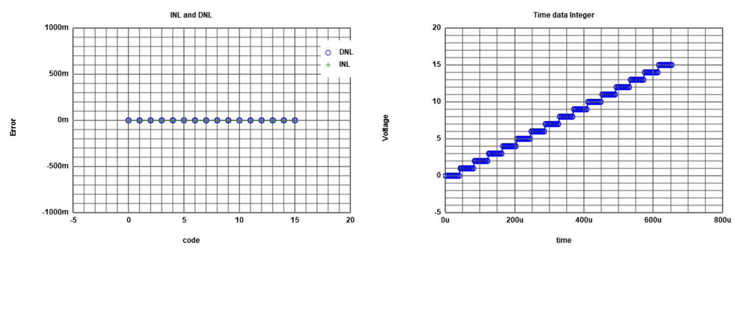
Here you can see the ideal ADC of a ramp signal. The ADC-DAC pipe is ideal, therefore the INL and DNL of this converter is always 0. The histogram is calculated and drawn by Read Raw File . This tool is given by Professor Vollrath. The start time remains at 0, the stop time will be set to the simulation end time of LTSpice: 655,36 µs, the time step will be set, so we can display a histogram: 5,12 µs |

|
Ramp signal - LSB
|
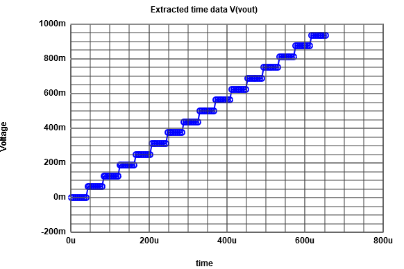
Afterwards the raw file of the simulated LTSpice Model is selected. With the formula the least significant bit can be calculated. |

|
Ramp signal non-ideal

|
Now the measurement will be executed with a non-ideal DAC. This should simulate real life application and should show the problems with ADC and DAC. You can see the high INL and DNL error because of the manipulated R6 and R9. They are set from: R6 = 1kΩ -> R6 = 1.3kΩ R9 = 2kΩ -> R9 = 1.5kΩ |
Sine signal ideal
|
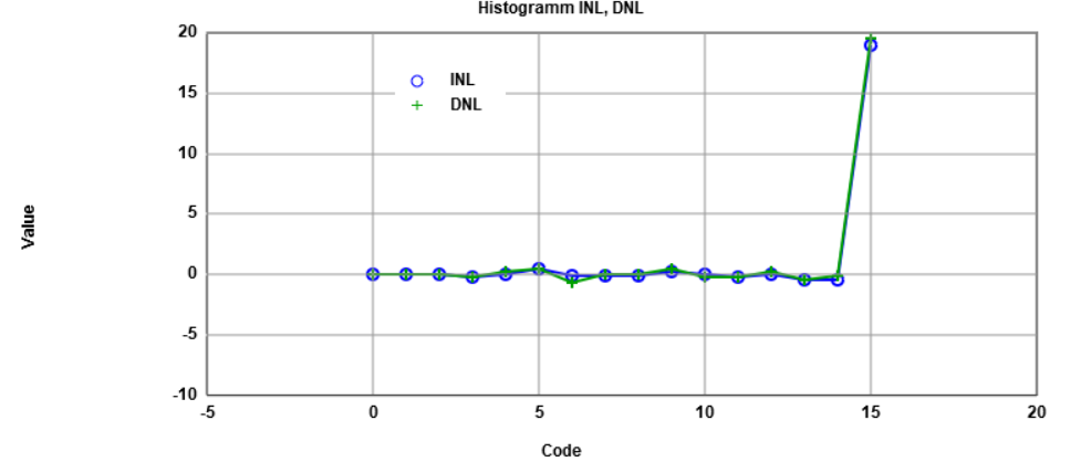
The same measurement will be executed with the sine signal. At first we will have a look at the ideal ADC DAC pipe. As you can see, the INL and DNL of the ideal ADC DAC pipe is close to 0. The last value of this curve is false because of the JavaScript implementation. |

|
Sine signal non-ideal
|
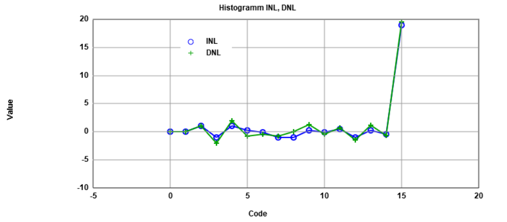
Again you can see here the non ideal ADC DAC with the high alternating INL and DNL error. Like above the last value is not correct due to a faulty JavaScript. |

|
Summary
Things learned
- Correlation between INL and DNL
- Operating a R2R DAC
- Extracting raw Files from LTSpice
- Implementing raw data to a histogram
Problems solved
- Saving the raw file in a seperate directory
to save file size from the zipped folder - Getting used to Web-page programming
References
[1] Making of a Webreport , Vollrath
[2] Laboratory 03: ADC DAC analysis instructions , Vollrath