Microelectronics08 System, Synthesis, VHDLProf. Dr. Jörg Vollrath07 CMOS Logic |
Video of lecture 09 (12.05.2021)
|
Länge: 1:30:00 |
0:0:0 Review 0:1:15 MOSFETs for other purposes 0:5:3 Function to layout 0:6:56 AOI style 0:12:45 Output capacitance and layout 0:16:56 Delay 0:20:16 Truth table 0:24:24 AOI design style 0:25:56 Sum of products (SOP) 0:30:17 Multiplexer, Demultiplexer and logic 0:39:16 Bigger truth table implementation 0:46:56 Tri-state driver 0:48:6 Chip layout 0:55:46 Design entry 1:0:49 Silicon compiler example 1:3:6 Tool chain 1:4:41 Silicon Compiler explore design space 1:6:31 Configurong silicon compiler 1:9:36 VHDL entity and ports 1:11:44 architecture, component, structural 1:15:4 Hierarchy and connection 1:18:37 Behavioral and structural VHDL 1:19:50 Wiring layers and area 1:22:40 VHDL overview |
Video of Multiplier (17.05.2021)
|
Länge: 1:30:00 |
0:0:0 Multiplier 0:2:14 Example 2 2 bit numbers 0:6:10 Design options 0:11:59 Inputs and outputs, equations 0:16:9 Add2 operation LUT26, LUT28 0:18:59 LUT26 naming convention 0:22:59 Start library multiplier 0:23:46 Schematic 0:30:39 Make icon 0:32:14 Hooking up the subcircuits 0:36:44 Simulation 0:39:39 SPICE text 0:41:1 Pulse statements 0:42:14 Simulate SPICE 1:18:4 Setting up waveform display 0:44:12 Check output 0:46:34 Generate reference output 0:48:14 Tool silicon compiler 0:50:34 Change text size 0:51:44 LTSPICE layout simulation |
Overview 2024
- Parasitics: R, C
- AOI design style
Today:
- Unit transistor
- Cell layout, adder, ALU, data path
- System synthesis
- VHDL entity and architecture
From VHDL to layout
Integrated circuit design methods
- Basic library: muddlib, sclib
- Manual place and route
- Automatic place and route from schematic
- Transfering behavioral VHDL to structural VHDL and automatic place and route
sclib.jelib and Xilinx Webpack with Spartan 3E, xc3s250, cp132
Data exchange is done through files.
Basic libraries
A library for a MIPS processor: muddlib07.jelibUsing "Silicon Compiler" with VHDL: sclib.jelib
Standard cell: NAND layout
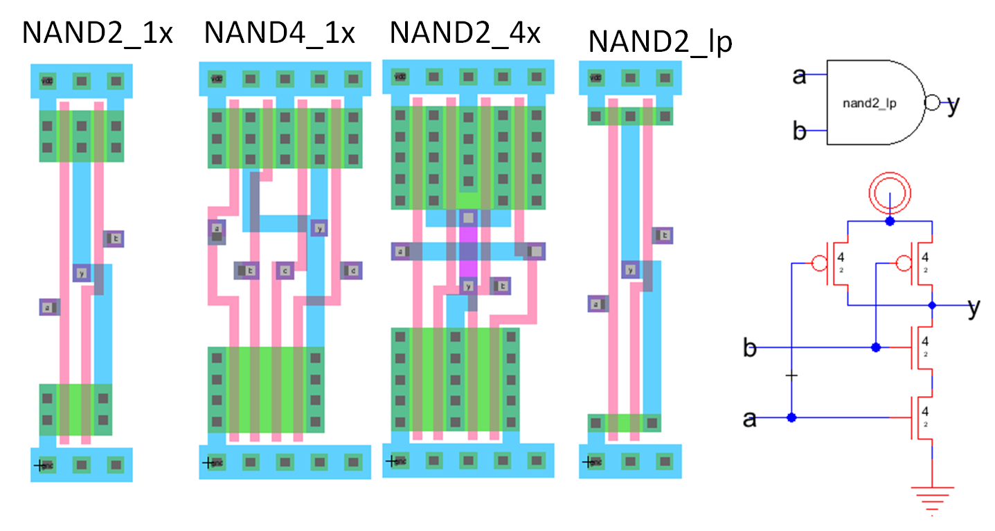
Cell Discussion:
Transistors
Width determined by number of input and outputs
Same height, names, vertical horizontal lines, exports, hierarchy
Layout 1-Bit Adder
|
library: muddlib_07 cell: fulladder pins: a, b, cin, sum, cout Very nice regular Not area optimized Standard cell
|
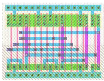 |
This is an example from a MIPS microprocessor.
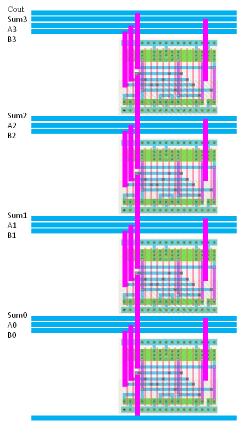
Multiple cells: 4 Bit Adder Floorplan
Use grid for wiring
|
 |
Manual planning, place and route for data path
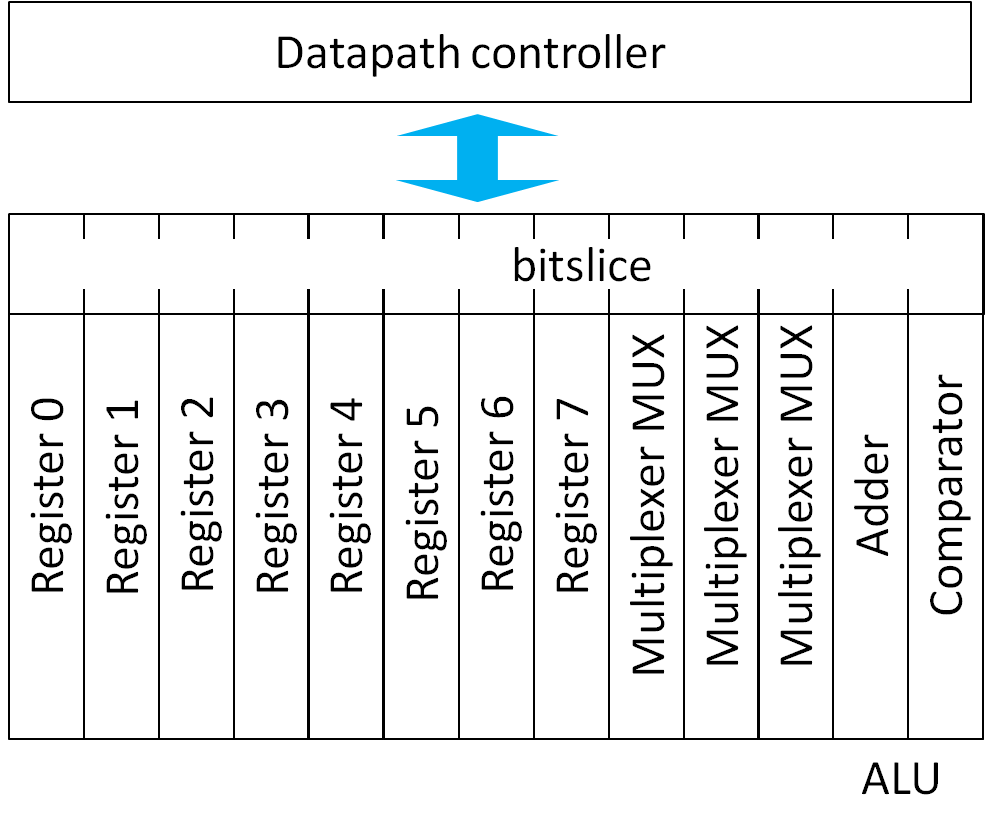
Control circuits are at the top.
For each bit a row (bitslice) is taken with functionality of register, mux, alu.
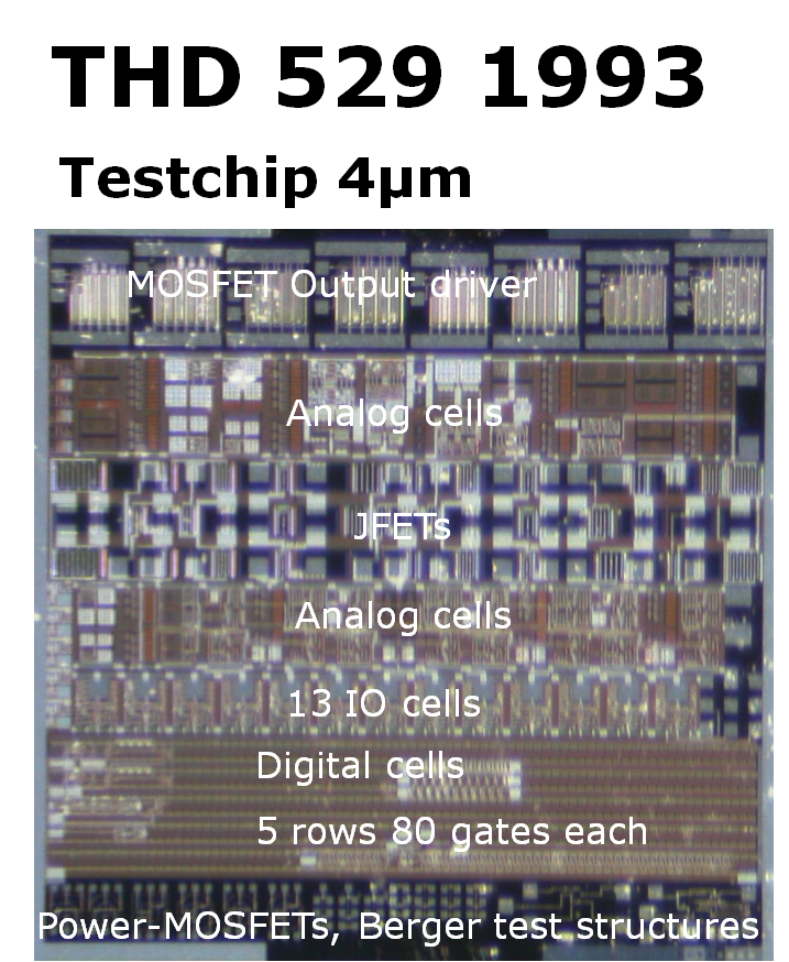
Chip layout
 |
 |
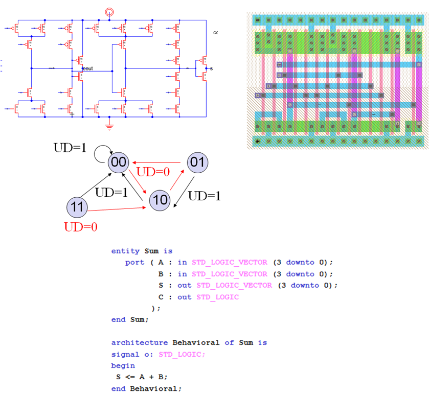
Design Entry
|
 |
Schematic and VHDL
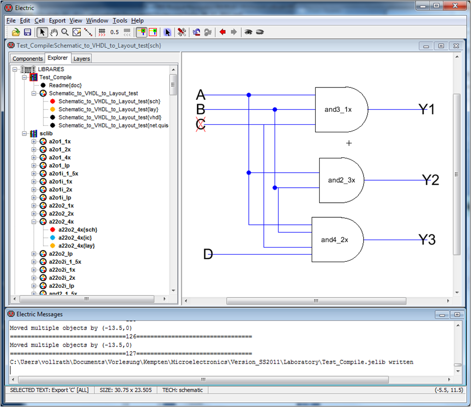
There are tools available to convert a schematic to layout.
This operation is called synthesis and in "VLSI Design System" a tool Silicon Compiler is used.
This tool needs basic layouts for transistors or logic cells which are available in sclib.jelib.
This library has to be loaded before using the Silicon Compiler.
Here a schematic of a typical logic circuit is shown. Each logic circuits has a layout.
The Silicon Compiler places the layout cells and does the wiring using M1 and M2.
The next slides shows the result and more detailed instructions to get the Silicon Compiler working without errors.
Engineering tools normally have some quirks and error messages and special procedures to overcome errors. Bug fix requests are often done, but seldom implemented due to successful workarounds.
A trained user will avoid these errors and stops complaining after a while.
An engineer should be aware of this and able to find workarounds.
Layout
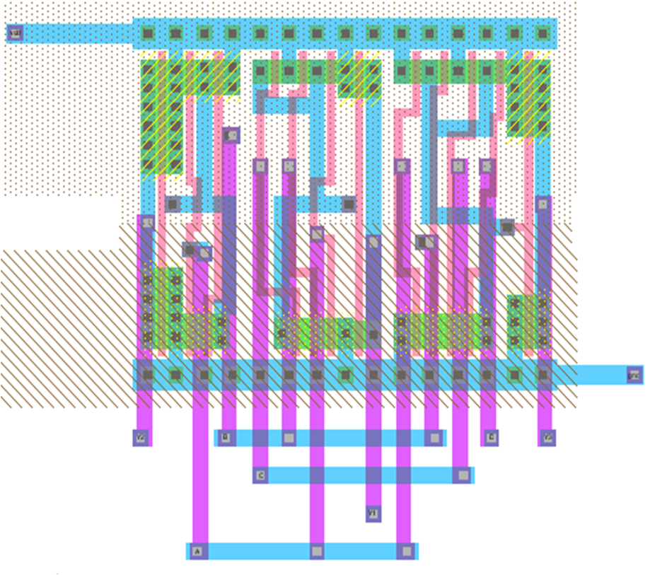
The picture shows the generated layout.
The wiring of logic cells is done by routing M2 wires vertically below the cells and connecting these wires with horizontally running M1 wires.
The wiring of logic cells is done by routing M2 wires vertically below the cells and connecting these wires with horizontally running M1 wires.
Wiring Layers and Area
 |
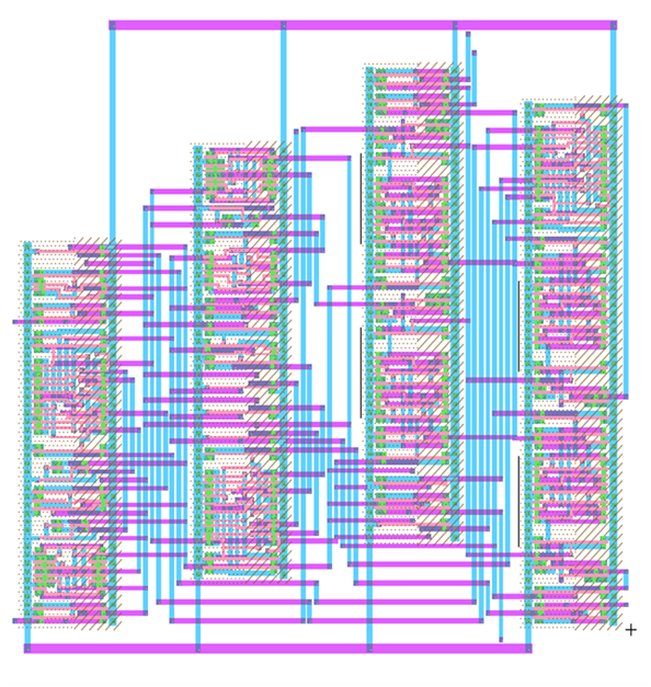 |
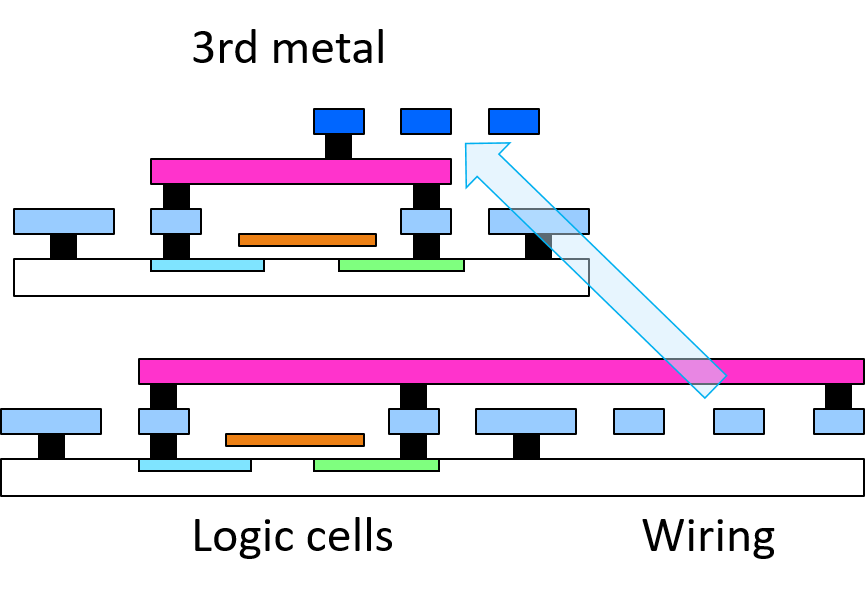
Light blue metal1 M1 lines are used vertically, M2 lines are used horizontally.
Between strips/columns of logic cells the M1, M2 routing is placed.
More area is used for wiring than for active devices.
Having more metal layers for routing allows putting wiring on top of logic cells.
This is shown on the cross section on the left side, where 2 M1 lines are placed as M3 lines on top and the width of the layout is reduced.
The layout was generated using a mod_m_counter layout.
Silicon Compiler Start
|
|
VHDL code relating to cells with layout in sclib (LUT2, MUX, FDC)
having nmos, pmos subcircuit in it, should be deleted.
Connections to vdd or gnd have to be modified, so that these are using vddx and gndx signals, which will be connected at the top level to vdd and gnd.
Connections to vdd or gnd have to be modified, so that these are using vddx and gndx signals, which will be connected at the top level to vdd and gnd.
Silicon Compiler Continued
|
|
Error:SC Maker cannot find Horizontal Arc Metal-1 in technology artwork
Select a metal arc in a layout
Then in Preferences, Tools, Silicon compiler, under Arcs:
Horizontal routing arc: Metal-1
Vertical routing arc: Metal-2
should appear.
Select a metal arc in a layout
Then in Preferences, Tools, Silicon compiler, under Arcs:
Horizontal routing arc: Metal-1
Vertical routing arc: Metal-2
should appear.
Silicon Compiler Finish
|
|
Design strategy
- Place and Route for schematics
- Netlist, Structural VHDL
- Hardware description language
- VHDL, Verilog
- Structural, Behavioral
- Digital Design: FPGA and ASIC
- Use known good blocks with test suites
- Limited number of used structures/blocks
Historically it was not clear, what integrated circuits will be realized.
Today basic blocks can be identified. They are listed top to bottom:
- Applications: uC, Audio/Videoprocessing, FFT, System Control, wireless communication
- Teaching: Reaction Timer, Traffic Light, Counter, (uP, UART, Filter, Control)
- Hardware System: uC (Arduino, ESP32, RasPi), FPGA (BASYS3, Altera, Lattice)
- Software System: OS, Service (websocket, AJAX), IDE (HTML, Javascript, C++, C, VHDL, Verilog)
- Hardware Digital Blocks: Memory, CPU, GPU, NPU, SERDES (SPI, I2C, CAN, USB, UART
- Hardware Analog Blocks: Bandgap Reference, Operational amplifier (Power, RailToRail), DC-DC, WIFI
- Analog-Digital: ADC, DAC
- State Blocks: Counter, SERDES, MACC, PID, ALU
- Logic Blocks: MUX, AOI, ADD, CMP, Truth table (Why?)
- CMOS Transistors: NFET, PFET, Inverter, Transmission Gate (MUX), NAND, DFF
VHDL versus Verilog
VHDL | Verilog |
| University | Industry |
| Europe | USA |
| Specific Syntax Prevents some errors early |
Easy Syntax Error detection later |
FPGA IDE covers both | |
| Classes Teaching | |
| Tiny Tapeout | |
VHDL overview
- What is VHDL?
- Strategy: Copy, paste, adapt
- Basic Block structure
- Keywords
- Hierarchy and Connection
- State machine
- Test vector
- Summary
You do not need to know all details of VHDL!
Copy, paste, modify
In former times a tool or programming language first was studied in detail and then examples were programmed.
Nowadays there are many working examples or libraries available using good coding style, good documentation and test benches.
Working examples are studied, copied, pasted and modified on a need to know basis.
VHDL examples should have the hardware code and a test bench with an expected output to be able to verify operation and understand the circuit.
VHDL Definition (Wikipedia)
- Hardware description language (HDL)
- Behavioral Description
- Internal optimization possible
- Translation code to hardware: Synthesis
- Resource:
http://en.wikipedia.org/wiki/VHDL
- How do we build logic functions?
- How do we build state machines?
- How do we test?
Tutorial Introduction to VHDL:
https://www.nandland.com/vhdl/tutorials/tutorial-introduction-to-vhdl-for-beginners.htmlBooks: Next Lecture
VHDL Block (Entity) and Logic (Architecture)
SUM = A + B
entity Sum is
   port ( A : in STD_LOGIC_VECTOR (3 downto 0);
          B : in STD_LOGIC_VECTOR (3 downto 0);
          S : out STD_LOGIC_VECTOR (3 downto 0);
          C : out STD_LOGIC
			 );
end Sum;

architecture Behavioral of Sum is
signal o: STD_LOGIC;
begin
 S <= A + B;
end Behavioral;
- Adder
- Entity
- Port
- In, out
- STD_LOGIC
- STD_LOGIC_VECTOR
- Architecture
- Signal
- Connection: <=
- Operation; +
Ports, Busses and Signals
- Input and Output of a circuit: Port
- In The signal can only be read (right side of connection)
- Out The signal can only be set (left side of connection)
- Buffer The signal can be read and set.
- Inout The signal can be read and set
- assignment: Y<= ‘0‘;
- Bus:
- STD_LOGIC_VECTOR, BIT_VECTOR
- MY_SHORT: in STD_LOGIC_VECTOR(3 downto 0);
- MY_SHORT <= “ 1101“;
- Individual Line: Y <= MY_WORD(2);
- MY_WORD <= MY_SHORT_1 & A & B & C; a bus consisting of some signals.
- Signal
- signal Y1, Y2: bit;
- Local lines can be set and read.
Verilog Block and Logic (module)
SUM = A + B
module sum(a,b,s,c);  // sum: s = a + b, c: carry
  input  [3:0] a;
  input  [3:0] b;
  output [3:0] s;
  output       c;

  wire [4:0] add;

 assign add = a + b;
 assign s = add[3:0];
 assign c = add[4];

endmodule
- Adder
- module and endmodule
- Ports
- input, output
- Bus: [3:0]
- Connection: assign
Three-state-driver
|
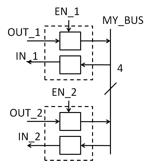 |
signal IN_1,OUT_1,IN_2, OUT_2, MY_BUS: std_logic_vector(3 downto 0);
Signal EN_1;EN_2:std_logic;
begin
IN_1 <= MY_BUS; IN_2 <= MY_BUS;
MY_BUS <= OUT_1 when EN_1= ‘1‘ else (others=>‘Z‘);
MY_BUS <= OUT_2 when EN_2= ‘1‘ else (others=>‘Z‘);
end Test;
Hierarchy and Connection (VHDL)
|
 |
Hierarchy and Connection (Verilog)
|
 |
State machine, process, incomplete if (VHDL)
Process
|
|
State machine (Verilog)
Process
|
|
Finite state machine in VHDL
Truth table: logic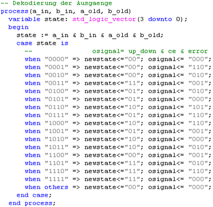 |
Register transfer
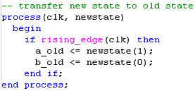 |
Library IEEE (VHDL)
|
|
Test and input signals (VHDL)
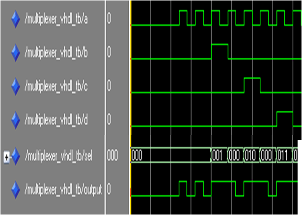 |
|
Test and input signals (Verilog)
 |
|
The timescale at the beginning of the file is defined.
After the initial statements the timing information #0 adds 0 to currrent time and the state information rst_n = 0; at this time is added.
Loops can make the life easier.
After the initial statements the timing information #0 adds 0 to currrent time and the state information rst_n = 0; at this time is added.
Loops can make the life easier.
Input signal timing (VHDL)
procedure VECTORTIMING (CLKi,S1i,S0i: in std_logic) is
-------------------------------------------------------------------------------
-- timing information for usage with synchronous designs and test
-------------------------------------------------------------------------------
 constant TCYCLE : Time := 100ns;                      -- cycle time

 begin
    CLK <= CLKi after (TCYCLE/2), '0'after (TCYCLE);   -- CLK pulse width
    S1 <= S1i   after 10ns, '0' after 70ns;
    S0 <= S0i   after 10ns, '0' after 70ns;
    wait for TCYCLE;                                   -- go to cycle end time
end procedure VECTORTIMING;

Begin
--     VECTORTIMING (CLKi,  S1i,  S0i );
------------------------------------------------------------------------
       VECTORTIMING ( '1',  '1',  '0‘ );
End;
Test and Timing simulation
High levelIRSIM
Measured delay times for blocks are used for timing calculation
Faster than transistor level simulation with transistor equation
There should be an expectation when signals should have a certain state/level
Prepare for test
Compare, pass, fail, number of errors
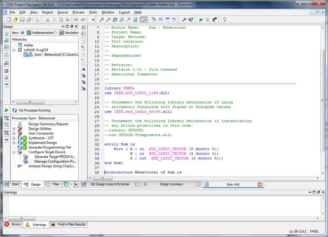
VHDL Design and Verification Environment
No costFPGA vendors: Altera, Xilinx
Old: Xilinx WebPack free to download
New: Xilinx Vivado free to download
Behavioral and structural VHDL
Behavioral
entity mod_m_counter is
   generic(
      N: integer := 4;     -- number of bits
      M: integer := 10     -- mod-M
  );
   port(
      clk, reset: in std_logic;
      max_tick: out std_logic;
      q: out std_logic_vector(N-1 downto 0)
   );
end mod_m_counter;

architecture arch of mod_m_counter is
   signal r_reg: unsigned(N-1 downto 0);
   signal r_next: unsigned(N-1 downto 0);
begin
   -- register
   process(clk,reset)
   begin
      if (reset='1') then
         r_reg <= (others=>'0');
      elsif (clk'event and clk='1') then
         r_reg <= r_next;
      end if;
   end process;
   -- next-state logic
   r_next <= (others=>'0') when r_reg=(M-1) else
             r_reg + 1;
   -- output logic
   q <= std_logic_vector(r_reg);
   max_tick <= '1' when r_reg=(M-1) else '0';
end arch;
Structural
entity LUT4_0DF0 is port( I0,I1,I2,I3: in STD_LOGIC;O: out STD_LOGIC);
end LUT4_0DF0;

architecture LUT4_0DF0_BODY of LUT4_0DF0 is
  component LUT20 port ( I0,I1 : in STD_LOGIC;O: out STD_LOGIC); end component;
  component LUT2D port ( I0,I1 : in STD_LOGIC;O: out STD_LOGIC); end component;
  component LUT2F port ( I0,I1 : in STD_LOGIC;O: out STD_LOGIC); end component;
  component MUX4 port(I0,I1,I2,I3,I4,I5 : in STD_LOGIC;O: out STD_LOGIC); end component;

  signal y1,y2,y3,y4,O2 : STD_LOGIC ;

begin
  LUT2_1: LUT20 port map (I0,I1,Y1);
  LUT2_2: LUT2F port map (I0,I1,Y2);
  LUT2_3: LUT2D port map (I0,I1,Y3);
  LUT2_4: LUT20 port map (I0,I1,Y4);
  MUX0: MUX4 port map (Y1,Y2,Y3,Y4,I2,I3,O);
end LUT4_0DF0_BODY;
ISE Webpack can be used to transfer behavioral VHDL in structural VHDL.
AnalyzeJS.html transfers the structural VHDL to Electric compatible VHDL.
Electric can then synthesize the circuit with elements of circuit sclib.jelib.
An example is synthesis of a UART.
Vivado can be used to transfer behavioral VHDL in structural VHDL.
AnalyzeJSV.html transfers the structural VHDL to Electric compatible VHDL.
After Synthesis run a command in the 'Tcl Console':
write_vhdl <filename>
A VHDL file using UNISIM components is generated.
A very basic FPGA like Arty S7-25 (xc7s25csga324-1) or BASYS3 board should be used to limit the variety of UNISIM components.
(FDRE, FDSE, IBUF, OBUF, LUT1, LUT6, BUFG, LUT2, LUT3, LUT4, LUT5, LUT6, CARRY4)
Implementation in sclib.jelib is done.
Summary VHDL
- Block description:
Entity, Architecture - Interface (port, in, out, inout) and wires (signal)
Std_logic, std_logic_vector - Logic function
Connection y <=a
Boolean function: y <= a & b; - State machine
Truth table: Process, case, if
Edge triggered: Rising_edge(clk) - Hierarchy:
Component, port map - Test:
Vectors and timing