DAC speed: voltage difference requirement
|
A capacitor has to be charged to the 1/2 LSB range of the input voltage: \( | V_e - V_a | < 0.5 LSB \) The voltage on the capacitor is: \( V_a = V_e \cdot \left( 1 - e^{-\frac{t}{\tau}} \right) \) with \( \tau = RC \) Maximum difference could be full scale \( V_e = 2^{B} \cdot LSB \) with B number of bits: \( 2^{B} \cdot LSB \cdot e^{-\frac{t}{\tau}} < 0.5 LSB \) \( -\frac{t}{\tau} < \left( -B-1 \right) ln \left( 2 \right) \) \( t > R C \left( B+1 \right) ln \left( 2 \right) \) |
|
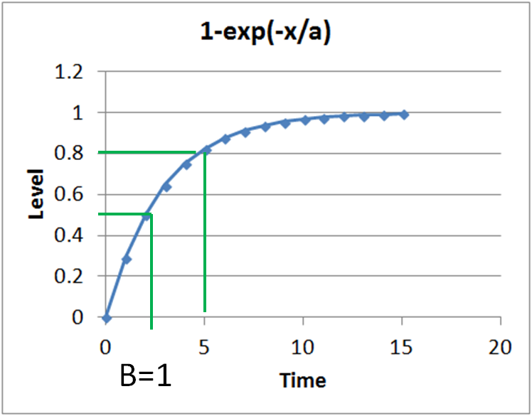
Settling time: (B+1)*t1
A capacitor has to be charged to the 1/2 LSB range of the input voltage:
\( | V_e - V_a | < 0.5 LSB \)
The voltage on the capacitor is:
\( V_a = V_e \cdot \left( 1 - exp^{-\frac{t}{\tau}} \right) \) with \( \tau = RC \)
This gives:
\( V_e - V_e \cdot \left( 1 - exp^{-\frac{t}{\tau}} \right) < 0.5 LSB \) \( V_e \cdot e^{-\frac{t}{\tau}} < 0.5 LSB \)
Maximum difference could be full scale \( V_e = 2^{B} \cdot LSB \) with B number of bits:
Measurement:
Time when half level is reached: t1
Settling time: (B+1)*t1
\( | V_e - V_a | < 0.5 LSB \)
The voltage on the capacitor is:
\( V_a = V_e \cdot \left( 1 - exp^{-\frac{t}{\tau}} \right) \) with \( \tau = RC \)
This gives:
\( V_e - V_e \cdot \left( 1 - exp^{-\frac{t}{\tau}} \right) < 0.5 LSB \) \( V_e \cdot e^{-\frac{t}{\tau}} < 0.5 LSB \)
Maximum difference could be full scale \( V_e = 2^{B} \cdot LSB \) with B number of bits:
| \( 2^{B} \cdot LSB \cdot exp^{-\frac{t}{\tau}} < 0.5 LSB \) | \( exp^{-\frac{t}{\tau}} < 2^{-B-1} \) | |
| \( -\frac{t}{\tau} < ln \left( 2^{-B-1} \right) \) | \( -\frac{t}{\tau} < \left( -B-1 \right) ln \left( 2 \right) \) | |
| \( t > R C \left( B+1 \right) ln \left( 2 \right) \) |
Measurement:
Time when half level is reached: t1
Settling time: (B+1)*t1
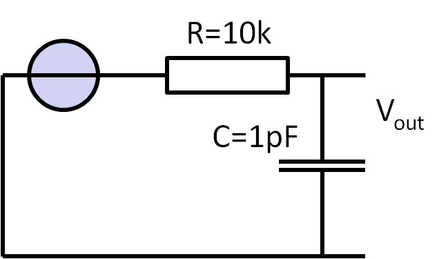
RC low pass thermal noise
|
A resistor has a noise voltage: \( \frac{V_{rms}^2}{\Delta f} = 4 k_B \cdot T \cdot R \) A low pass RC network limits the noise to: \( \overline{v_n^2} = \frac{k_B T}{C} \) This noise has to be lower than the quantization noise: \( \overline{v_q^2} = \frac{\Delta^2}{12} = \frac{V_{FS}^2}{2^{2B} \cdot 12}\) \( \frac{k_B T}{C} \lt \frac{V_{FS}^2}{2^{2B} \cdot 12}\) \( \frac{C}{k_B T} \gt \frac{2^{2B} \cdot 12}{V_{FS}^2} \) |
|
Elektronik 3: 24 Rauschen
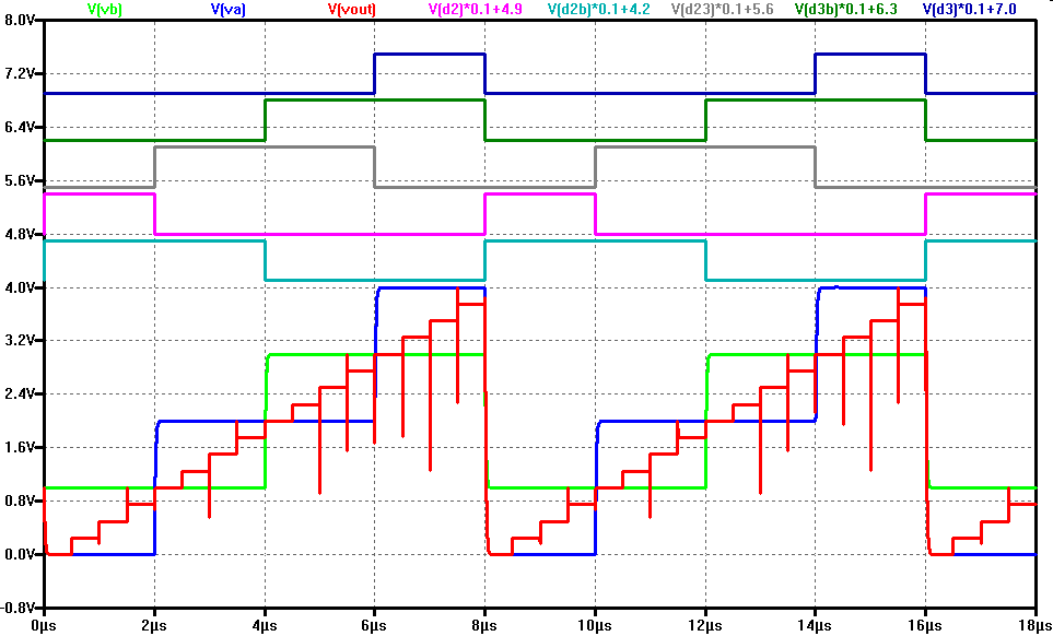
4 Bit interpolating R string, ladder DAC
|
Extra logic is needed to generate the control signals from the binary input code.
2 switches are always active on the left side for the 2 high order bits providing an upper and lower voltage for interpolation.
The simulation shows the control signals for the upper bits, the intermediate voltages VA and VB and the resulting output voltage Vout.
2 switches are always active on the left side for the 2 high order bits providing an upper and lower voltage for interpolation.
The simulation shows the control signals for the upper bits, the intermediate voltages VA and VB and the resulting output voltage Vout.
| MSB DA3 | DA2 | DA1 | LSB DA0 |
D3 | D3b | D23 | D2b | D2 | D1 | D1b | D01 | D0 | D0B | VA/V | VB/V |
| 0 | 0 | 0 | 0 | 0 | 0 | 0 | 1 | 1 | 1 | 0 | 0 | 0 | 1 | 0 | 1 |
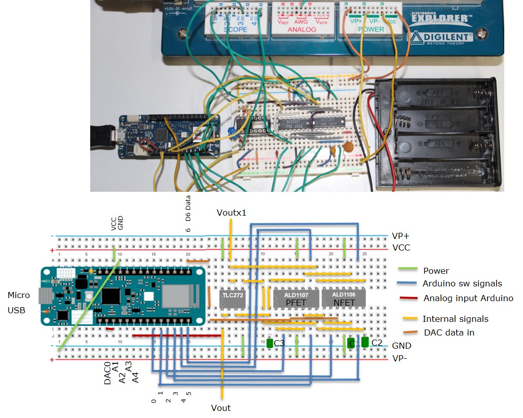
Low Cost Serial C DAC Circuit
|
Simulation schematic LTSPICE Minimum number of parts Number of cycles gives the resolution Low cost Arduino MKR WIFI1010 TLC272 ALD1106, ALD1107 3x C=20nF Breadboard Study DAC simulation, measurement, errors and error correction |
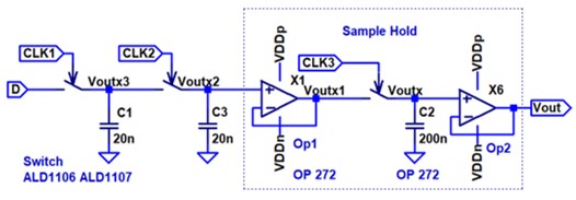  |
\( Voutx2(n+1) = \frac{Voutx2(n) + Voutx3}{2}
= \frac{Voutx2(n) + VDD \cdot D(n)}{2} \)
\( Voutx2(n+1) = VDD \cdot (0.25 \cdot Voutx2(n-1) + 0.25 \cdot D(n-1) + 0.5 \cdot D(n) \)
\( Vout = \sum_{k=0}^{nBit-1} 2^{-nBit+k} D(k) \)
Vollrath, "Low cost serial DAC", MPC Workshop, 2024
\( Voutx2(n+1) = VDD \cdot (0.25 \cdot Voutx2(n-1) + 0.25 \cdot D(n-1) + 0.5 \cdot D(n) \)
\( Vout = \sum_{k=0}^{nBit-1} 2^{-nBit+k} D(k) \)
Vollrath, "Low cost serial DAC", MPC Workshop, 2024