Loading [MathJax]/extensions/tex2jax.js
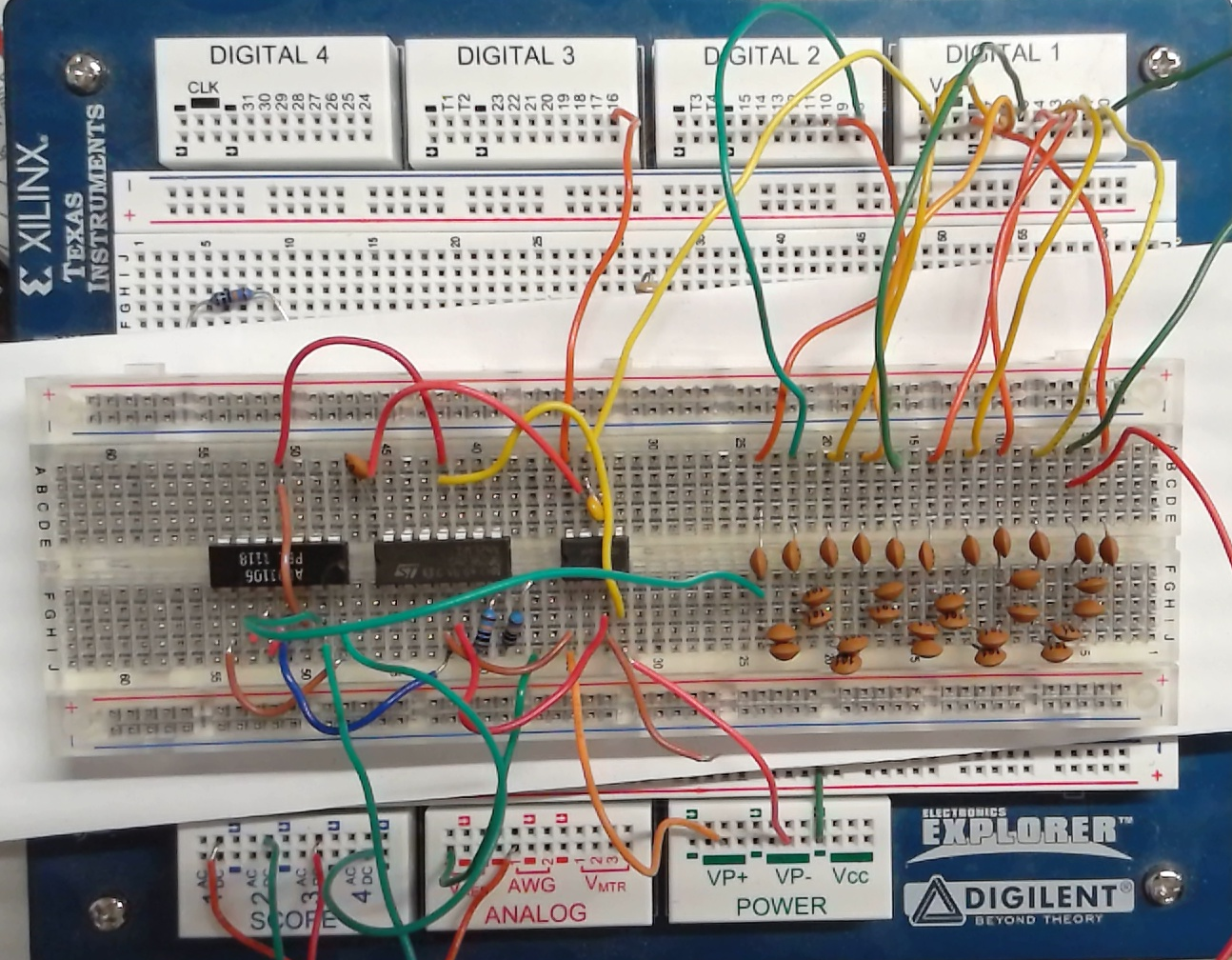
Laboratory 4: Measuring a 10 Bit C2C DAC
Components:
1 x Breadboard
22 x Capacitors (10 pF, 100 pF, 1 nF)
Amplifier and sample and hold:
1 x LF398
1 x LM324
1 x ALD1106
1 x ALD1107
2 x Resistors 100 kΩ
Easy wiring:
5 x 12 Pin connectors
|
|
Task:
There will be 3 parts:
- Characterize measurement equipment.
- Measure static and dynamic performance of a C2C-DAC.
Experience measurement problems and learn how to improve INL and DNL by circuit adjustments
and digital assistance.
- Use an opamp and a sample and hold
This is an open laboratory extending until 21.1.2019. Report will be due 25.1.2019.
1. Characterize measurement equipment.
Measurement equipment:
For measurements the Electronic Explorer board is used:
Operation of Electronic Explorers
Set up:
Connect AWG 1 with SCOPE OSC1 DC to estimate the INL, DNL and signal to noise of the
waveform generator and the oscilloscope.
Details:
Start the oscilloscope and the arbitrary waveform generator.
Select a sine signal with a frequency of 53.71749481 kHz an amplitude of 2 V and an offset of 2 V.
For channel 1 select a time range of 2 µs per division, range of 500 mV/div and offset of -2 V.
Creat a math function generating positive integer values: round(C1 * 2* 1024 + 200).
Check with the vertical minimum function of M1 that all values are positive.
Display only the positive integer values. Export the values.
Source: Main Time, Type: Comma Separated Values, Untick Save Options Comments, Header and Label.
Copy the integer data to the clipboard.
Copy the integer values into the input field of the FFT, INL, DNL tool:
FFT_Javascript_2017_Calibration.html
Do 'Read positive integer data'.
Set the number of points to 8192 and the number of bits to 12.
Do 'Generate Charts'.
Check the input signal for number of periods and range.
What is the signal to noise, INL and DNL value.
What is the maximum number of bits, which can be measured?
Discuss your results, document your challenges and results.
Make screenshots of the FFT analysis.
2. Measure static and dynamic performance of a C2C-DAC.
Build a 10-Bit C2C DAC according to the circuit below using only the operational
amplifier LM324, not yet the sample and hold LF398 and connect
it with the Electronic Explorer.
Details:
Data inputs and switches are realized with DIGITAL1 0..7 and DIGITAL2 8,9.
DIGITAL3,4 22-31 will be later used as oscilloscope trigger signal.
DIGITAL2 12 will be later used for the sample and hold CLK.
AWG1 is connected as Voffset to shift the output to positive values.
SCOPE: OSC1 trigger DIGITAL2 9 or later Digital4 31.
SCOPE: OSC2 vint.
SCOPE: OSC3 vout.
SCOPE: OSC4 for monitoring other nodes and later Vout1.
VP+ = 4 V is used as positive voltage for the opamp.
VP- = -4 V is used as negative voltage for the opamp.
All GND pins (Bold dash or small white arrow on colored background) are
connected on the Electronic Explorer.
Version 4
SHEET 1 1884 680
WIRE -416 -80 -560 -80
WIRE -304 -80 -416 -80
WIRE -208 -80 -304 -80
WIRE -96 -80 -208 -80
WIRE 16 -80 -96 -80
WIRE 128 -80 16 -80
WIRE 256 -80 128 -80
WIRE 368 -80 256 -80
WIRE 480 -80 368 -80
WIRE 592 -80 480 -80
WIRE 752 -80 592 -80
WIRE -560 -64 -560 -80
WIRE -384 -64 -496 -64
WIRE -272 -64 -384 -64
WIRE -176 -64 -272 -64
WIRE -64 -64 -176 -64
WIRE 48 -64 -64 -64
WIRE 160 -64 48 -64
WIRE 288 -64 160 -64
WIRE 400 -64 288 -64
WIRE 512 -64 400 -64
WIRE 624 -64 512 -64
WIRE -416 -48 -416 -80
WIRE -384 -48 -384 -64
WIRE -304 -48 -304 -80
WIRE -272 -48 -272 -64
WIRE -208 -48 -208 -80
WIRE -176 -48 -176 -64
WIRE -96 -48 -96 -80
WIRE -64 -48 -64 -64
WIRE 16 -48 16 -80
WIRE 48 -48 48 -64
WIRE 128 -48 128 -80
WIRE 160 -48 160 -64
WIRE 256 -48 256 -80
WIRE 288 -48 288 -64
WIRE 368 -48 368 -80
WIRE 400 -48 400 -64
WIRE 480 -48 480 -80
WIRE 512 -48 512 -64
WIRE 592 -48 592 -80
WIRE 624 -48 624 -64
WIRE -496 -32 -496 -64
WIRE -496 -32 -624 -32
WIRE -368 -16 -368 -96
WIRE -256 -16 -256 -96
WIRE -160 -16 -160 -96
WIRE -48 -16 -48 -96
WIRE 64 -16 64 -96
WIRE 176 -16 176 -96
WIRE 304 -16 304 -96
WIRE 416 -16 416 -96
WIRE 528 -16 528 -96
WIRE 640 -16 640 -96
WIRE -400 48 -400 32
WIRE -288 48 -288 32
WIRE -192 48 -192 32
WIRE -80 48 -80 32
WIRE 32 48 32 32
WIRE 144 48 144 32
WIRE 272 48 272 32
WIRE 384 48 384 32
WIRE 496 48 496 32
WIRE 608 48 608 32
WIRE 752 48 752 -80
WIRE -656 96 -704 96
WIRE -656 112 -656 96
WIRE -704 160 -704 96
WIRE -704 160 -720 160
WIRE -800 176 -864 176
WIRE -784 176 -800 176
WIRE -464 176 -512 176
WIRE -400 176 -400 112
WIRE -400 176 -464 176
WIRE -384 176 -400 176
WIRE -288 176 -288 112
WIRE -288 176 -320 176
WIRE -272 176 -288 176
WIRE -192 176 -192 112
WIRE -192 176 -208 176
WIRE -176 176 -192 176
WIRE -80 176 -80 112
WIRE -80 176 -112 176
WIRE -64 176 -80 176
WIRE 32 176 32 112
WIRE 32 176 0 176
WIRE 48 176 32 176
WIRE 144 176 144 112
WIRE 144 176 112 176
WIRE 176 176 144 176
WIRE 272 176 272 112
WIRE 272 176 240 176
WIRE 288 176 272 176
WIRE 384 176 384 112
WIRE 384 176 352 176
WIRE 400 176 384 176
WIRE 496 176 496 112
WIRE 496 176 464 176
WIRE 512 176 496 176
WIRE 608 176 608 112
WIRE 608 176 576 176
WIRE 640 176 608 176
WIRE 752 176 752 112
WIRE 752 176 704 176
WIRE -688 192 -720 192
WIRE -672 192 -688 192
WIRE -576 192 -592 192
WIRE -496 208 -512 208
WIRE -576 240 -576 192
WIRE -496 240 -496 208
WIRE -496 240 -576 240
WIRE -800 256 -800 176
WIRE -784 256 -800 256
WIRE -688 256 -688 192
WIRE -688 256 -704 256
WIRE -400 272 -400 176
WIRE -384 272 -400 272
WIRE -288 272 -288 176
WIRE -288 272 -320 272
WIRE -272 272 -288 272
WIRE -192 272 -192 176
WIRE -192 272 -208 272
WIRE -176 272 -192 272
WIRE -80 272 -80 176
WIRE -80 272 -112 272
WIRE -64 272 -80 272
WIRE 32 272 32 176
WIRE 32 272 0 272
WIRE 48 272 32 272
WIRE 144 272 144 176
WIRE 144 272 112 272
WIRE 176 272 144 272
WIRE 272 272 272 176
WIRE 272 272 240 272
WIRE 288 272 272 272
WIRE 384 272 384 176
WIRE 384 272 352 272
WIRE 400 272 384 272
WIRE 496 272 496 176
WIRE 496 272 464 272
WIRE 512 272 496 272
WIRE 608 272 608 176
WIRE 608 272 576 272
WIRE 640 272 608 272
WIRE 752 272 752 176
WIRE 752 272 704 272
WIRE -688 304 -688 256
WIRE -672 304 -688 304
WIRE -544 304 -592 304
WIRE -624 512 -624 480
WIRE -640 528 -704 528
WIRE -560 528 -608 528
WIRE -480 528 -560 528
WIRE -560 544 -560 528
WIRE -560 624 -560 608
FLAG -864 176 Vout
IOPIN -864 176 Out
FLAG -624 -32 Vref
IOPIN -624 -32 In
FLAG -560 -64 0
FLAG 416 -96 D2
IOPIN 416 -96 In
FLAG 528 -96 D1
IOPIN 528 -96 In
FLAG 640 -96 D0
IOPIN 640 -96 In
FLAG -464 176 Vint
FLAG 304 -96 D3
IOPIN 304 -96 In
FLAG -48 -96 D6
IOPIN -48 -96 In
FLAG 64 -96 D5
IOPIN 64 -96 In
FLAG 176 -96 D4
IOPIN 176 -96 In
FLAG -160 -96 D7
IOPIN -160 -96 In
FLAG -256 -96 D8
IOPIN -256 -96 In
FLAG -368 -96 D9
IOPIN -368 -96 In
FLAG -544 304 Voffset
FLAG -656 112 0
FLAG -560 624 0
FLAG -480 528 Vout1
IOPIN -480 528 Out
FLAG -624 480 CLK
FLAG -704 528 Vout
IOPIN -704 528 In
SYMBOL cap 400 112 R180
WINDOW 0 24 56 Left 2
WINDOW 3 24 8 Left 2
SYMATTR InstName C10
SYMATTR Value 10p
SYMBOL cap 512 112 R180
WINDOW 0 24 56 Left 2
WINDOW 3 24 8 Left 2
SYMATTR InstName C7
SYMATTR Value 10p
SYMBOL cap 624 112 R180
WINDOW 0 24 56 Left 2
WINDOW 3 24 8 Left 2
SYMATTR InstName C4
SYMATTR Value 10p
SYMBOL Switch2 608 -16 R90
SYMATTR InstName X1
SYMBOL Switch2 496 -16 R90
SYMATTR InstName X2
SYMBOL Switch2 384 -16 R90
SYMATTR InstName X3
SYMBOL cap 400 192 R270
WINDOW 0 32 32 VTop 2
WINDOW 3 0 32 VBottom 2
SYMATTR InstName C8
SYMATTR Value 10p
SYMBOL cap 288 112 R180
WINDOW 0 24 56 Left 2
WINDOW 3 24 8 Left 2
SYMATTR InstName C13
SYMATTR Value 10p
SYMBOL Switch2 272 -16 R90
SYMATTR InstName X6
SYMBOL cap 768 112 R180
WINDOW 0 24 56 Left 2
WINDOW 3 24 8 Left 2
SYMATTR InstName C1
SYMATTR Value 10p
SYMBOL cap 640 192 R270
WINDOW 0 32 32 VTop 2
WINDOW 3 0 32 VBottom 2
SYMATTR InstName C2
SYMATTR Value 10p
SYMBOL cap 512 192 R270
WINDOW 0 32 32 VTop 2
WINDOW 3 0 32 VBottom 2
SYMATTR InstName C5
SYMATTR Value 10p
SYMBOL cap 288 192 R270
WINDOW 0 32 32 VTop 2
WINDOW 3 0 32 VBottom 2
SYMATTR InstName C11
SYMATTR Value 10p
SYMBOL cap 288 288 R270
WINDOW 0 32 32 VTop 2
WINDOW 3 0 32 VBottom 2
SYMATTR InstName C12
SYMATTR Value 10p
SYMBOL cap 400 288 R270
WINDOW 0 32 32 VTop 2
WINDOW 3 0 32 VBottom 2
SYMATTR InstName C9
SYMATTR Value 10p
SYMBOL cap 512 288 R270
WINDOW 0 32 32 VTop 2
WINDOW 3 0 32 VBottom 2
SYMATTR InstName C6
SYMATTR Value 10p
SYMBOL cap 640 288 R270
WINDOW 0 32 32 VTop 2
WINDOW 3 0 32 VBottom 2
SYMATTR InstName C3
SYMATTR Value 10p
SYMBOL cap -64 112 R180
WINDOW 0 24 56 Left 2
WINDOW 3 24 8 Left 2
SYMATTR InstName C22
SYMATTR Value 10p
SYMBOL cap 48 112 R180
WINDOW 0 24 56 Left 2
WINDOW 3 24 8 Left 2
SYMATTR InstName C19
SYMATTR Value 10p
SYMBOL cap 160 112 R180
WINDOW 0 24 56 Left 2
WINDOW 3 24 8 Left 2
SYMATTR InstName C16
SYMATTR Value 10p
SYMBOL Switch2 144 -16 R90
SYMATTR InstName X4
SYMBOL Switch2 32 -16 R90
SYMATTR InstName X5
SYMBOL Switch2 -80 -16 R90
SYMATTR InstName X7
SYMBOL cap -64 192 R270
WINDOW 0 32 32 VTop 2
WINDOW 3 0 32 VBottom 2
SYMATTR InstName C20
SYMATTR Value 10p
SYMBOL cap -176 112 R180
WINDOW 0 24 56 Left 2
WINDOW 3 24 8 Left 2
SYMATTR InstName C25
SYMATTR Value 10p
SYMBOL Switch2 -192 -16 R90
SYMATTR InstName X8
SYMBOL cap 176 192 R270
WINDOW 0 32 32 VTop 2
WINDOW 3 0 32 VBottom 2
SYMATTR InstName C14
SYMATTR Value 10p
SYMBOL cap 48 192 R270
WINDOW 0 32 32 VTop 2
WINDOW 3 0 32 VBottom 2
SYMATTR InstName C17
SYMATTR Value 10p
SYMBOL cap -176 192 R270
WINDOW 0 32 32 VTop 2
WINDOW 3 0 32 VBottom 2
SYMATTR InstName C23
SYMATTR Value 10p
SYMBOL cap -176 288 R270
WINDOW 0 32 32 VTop 2
WINDOW 3 0 32 VBottom 2
SYMATTR InstName C24
SYMATTR Value 10p
SYMBOL cap -64 288 R270
WINDOW 0 32 32 VTop 2
WINDOW 3 0 32 VBottom 2
SYMATTR InstName C21
SYMATTR Value 10p
SYMBOL cap 48 288 R270
WINDOW 0 32 32 VTop 2
WINDOW 3 0 32 VBottom 2
SYMATTR InstName C18
SYMATTR Value 10p
SYMBOL cap 176 288 R270
WINDOW 0 32 32 VTop 2
WINDOW 3 0 32 VBottom 2
SYMATTR InstName C15
SYMATTR Value 10p
SYMBOL cap -272 112 R180
WINDOW 0 24 56 Left 2
WINDOW 3 24 8 Left 2
SYMATTR InstName C28
SYMATTR Value 10p
SYMBOL Switch2 -288 -16 R90
SYMATTR InstName X9
SYMBOL cap -272 192 R270
WINDOW 0 32 32 VTop 2
WINDOW 3 0 32 VBottom 2
SYMATTR InstName C26
SYMATTR Value 10p
SYMBOL cap -384 112 R180
WINDOW 0 24 56 Left 2
WINDOW 3 24 8 Left 2
SYMATTR InstName C31
SYMATTR Value 10p
SYMBOL Switch2 -400 -16 R90
SYMATTR InstName X10
SYMBOL cap -384 192 R270
WINDOW 0 32 32 VTop 2
WINDOW 3 0 32 VBottom 2
SYMATTR InstName C29
SYMATTR Value 10p
SYMBOL cap -384 288 R270
WINDOW 0 32 32 VTop 2
WINDOW 3 0 32 VBottom 2
SYMATTR InstName C30
SYMATTR Value 10p
SYMBOL cap -272 288 R270
WINDOW 0 32 32 VTop 2
WINDOW 3 0 32 VBottom 2
SYMATTR InstName C27
SYMATTR Value 10p
SYMBOL res -576 176 R90
WINDOW 0 0 56 VBottom 2
WINDOW 3 32 56 VTop 2
SYMATTR InstName R1
SYMATTR Value 100k
SYMBOL res -576 288 R90
WINDOW 0 0 56 VBottom 2
WINDOW 3 32 56 VTop 2
SYMATTR InstName R2
SYMATTR Value 100k
SYMBOL Opamp2 -544 192 M0
SYMATTR InstName X11
SYMATTR Value opamp2
SYMATTR SpiceLine Aol=100K
SYMATTR SpiceLine2 GBW=10Meg
SYMBOL Opamp2 -752 176 M0
SYMATTR InstName X12
SYMATTR Value opamp2
SYMATTR SpiceLine Aol=100K
SYMATTR SpiceLine2 GBW=10Meg
SYMBOL res -688 240 R90
WINDOW 0 0 56 VBottom 2
WINDOW 3 32 56 VTop 2
SYMATTR InstName R3
SYMATTR Value 100k
SYMBOL cap -576 544 R0
SYMATTR InstName C32
SYMATTR Value 1n
SYMBOL SampleHoldCD -624 528 R0
SYMATTR InstName X13
TEXT -32 616 Left 2 !.model CD4007N NMOS(LEVEL=1 KP=1123u VT0=0.5 LAMBDA=0.018)\n.model CD4007P PMOS(LEVEL=1 KP=1123u VT0=-0.5 LAMBDA=0.018)
TEXT -80 352 Left 2 !.global VDD\n.include opamp2.sub\nV0 reset 0 PULSE(-1 5 0 1n 1n 499n 16000n)\nV1 d0 0 PULSE(5 -1 0n 1n 1n 999n 2000n)\nV2 d1 0 PULSE(5 -1 0 1n 1n 1999n 4000n)\nV3 d2 0 PULSE(5 -1 0 1n 1n 3999n 8000n)\nV4 d3 0 PULSE(5 -1 0 1n 1n 7999n 16000n)\nV5 d4 0 PULSE(5 -1 0 1n 1n 15999n 32000n)
TEXT -208 376 Right 2 !.tran 0 1024000n 100n 300n
TEXT 432 360 Left 2 !V6 d5 0 PULSE(5 -1 0 1n 1n 31999n 64000n)\nV7 d6 0 PULSE(5 -1 0 1n 1n 63999n 128000n)\nV8 d7 0 PULSE(5 -1 0 1n 1n 127999n 256000n)\nV9 d8 0 PULSE(5 -1 0 1n 1n 255999n 512000n)\nV10 d9 0 PULSE(5 -1 0 1n 1n 511999n 1024000n)\nVref Vref 0 DC 4\nVoffset Voffset 0 DC -4\nVDD VDD 0 DC 4\nVCLK CLK 0 PULSE(5 0 250n 1n 1n 500n 2000n)
TEXT -472 8 Right 2 !*.save V(vout)
TEXT -504 128 Left 2 ;10
TEXT -488 216 Left 2 ;9
TEXT -592 168 Left 2 ;8
TEXT -640 72 Left 2 ;LM324
TEXT -696 144 Left 2 ;12
TEXT -720 216 Left 2 ;13
TEXT -856 128 Left 2 ;14
TEXT -656 408 Left 2 ;LF398
TEXT -848 72 Left 2 ;4 VPP+
TEXT -880 328 Left 2 ;11 VPP-
TEXT -784 424 Left 2 ;1 VP+
TEXT -488 416 Left 2 ;4 VP-
TEXT -784 488 Left 2 ;3 input
TEXT -480 488 Left 2 ;5 output
TEXT -592 504 Left 2 ;6 Cs
TEXT -528 640 Left 2 ;7 logic ref GND
TEXT -608 448 Left 2 ;8 CLK
TEXT -784 616 Left 2 ;2 open
TEXT -288 416 Left 2 !.save V(Vint)
TEXT -360 456 Left 2 !.options plotwinsize=0
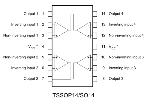
Operational amplifier LM324:
|
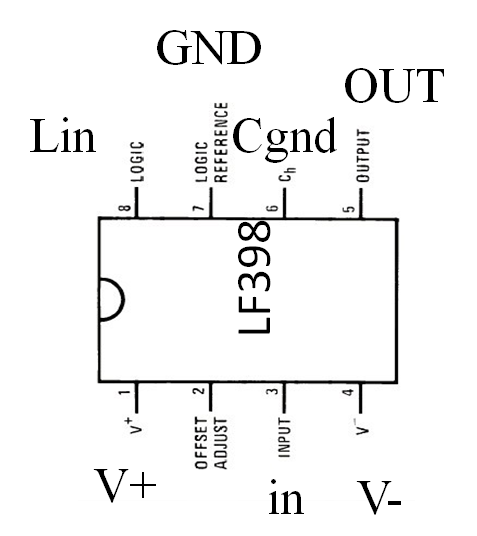
Sample and hold LF398:

|
Make a photo of your setup connected to the electronic explorer.
Start Waveforms.
Start the oscilloscope: Scope
Start the digital Patterns
Select DI0..DI10 as bus and counter.
Select voltage to control VP+ and VP-.
Ramp and sine measurement of the DAC:
Generate a binary counter pattern with the pattern generator and look
with the oscilloscope at the output of the 10-bit DAC.
- Measure the capacitance value of each capacitance with a multi meter.
Name | C1 | C2 | C3 | C4 | C5 | C6 | C7 |
C8 | C9 | C10 | C11 | C12 |
C [pF] | | | | | | | |
| | | | |
Name | C13 | C14 | C15 | C16 | C17 | C18 | C19 |
C20 | C21 | C22 | C23 | C24 |
C [pF] | | | | | | | |
| | | | |
Name | C25 | C26 | C27 | C28 | C29 | C30 | C31 |
C [pF] | | | | | | | |
- What is the offset, maximum voltage, LSB and settling time of the DAC?
Measure the signal Vint (after the DAC and before the opamp) and Vout (after the opamp).
Details:
Open the 'Patterns' window.
Create a bus with D[0]..D[9].
Use the type binary counter, output PP.
Select a frequency of 10 MHz, 1 MHz, 100 kHz, 10 kHz under 'parameter' for the counter.
Connect the MSB to OSC 1 DC as a trigger signal.
Connect the output of the DAC to OSC2 DC and change the counter frequency until you have a sawtooth curve.
Make sure that the settling time of the signal is ok for a full level transition.
Use the full vertical range of the oscilloscope to minimize error.
Channel 1 should show D9, channel 2 and 3 should show the output voltage before and after the opamp.
measure the settling time using a '00..0', '11..1' pattern:
Details:
Open the 'Patterns' window.
Select clock for the bus with values of 0 and 1023.
Vary the clock frequency.
Select clock for the bus with values of 511 and 512.
Vary the clock frequency.
Measure the settling time and switching noise of Vint and Vout.
Document challenges, effort and results and discuss your results.
- Measure and extract INL and DNL using
ReadOsci.html
Details:
With the oscilloscope do export data.
Copy the data into the 'input data' field.
Make sure to measure a positive ramp.
Set 'DNL, INL start', 'DNL, INL averaging length', 'DNL, INL step' and 'DNL, INL number of values' to appropriate values.
Set option for measurement analysis to 'Ramp INL, DNL'.
Do 'Process oscilloscope data'.
Document and discuss the result.
Select a frequency of 10 MHz, 1 MHz, 100 kHz, 10 kHz under 'parameter' for the counter.
What is the best frequency for the pattern generator for operation?
Document challenges, effort and results and discuss your results.
- Select the best frequency from the previous task.
Can you improve the INL and DNL of the transfer characteristic by changing capacitors?
Measure the improved circuit.
Document the improved capacitance values.
Document challenges, effort and results and discuss your results.
- Use a digital sine input and measure signal to noise ratio using a fft.
Import 10Bit_Sine43Periods.csv
into the pattern generator of the Electronic Explorer.
Details generating a sine signal:
New calibrated ramp data is loaded into the digital pattern generator with Type: Custom, Output: PP,
Edit: Parameters, Import file, open file, Browse, Ok, Import.
Import 10Bit_Sine1Period.csv
into the pattern generator of the Electronic Explorer.
You can use DDS_Sim_Javascript_2016.html
to generate other digital sine signals.
Measure with different signal frequencies and analyze data with
FFT_Javascript_2017_Calibration.html .
Document challenges, effort and results and discuss your results.
- Use ReadOsci.html
to calculate a calibration lookup table and generate a better ramp
DDS_Sim_Javascript_2016.html and sine signal.
Details, Step by Step:
1) Start with DDS Javascript and fill 0..1023 into Calibration and do 'Ramp EE vector with calibration'
2) Save the generated vectors on the drive and import them into the digital pattern generator:
type custom, edit parameters, Import file, open file, browse ok import
3) Measure the ramp with the oscilloscope and export the data
4) Do ReadOsci.html
and do 'Digital calibrated INL, DNL'
The calibration data appear at the bottom
5) Copy the calibration data into the DDS Javascript Calibration data and generate 1024 vectors.
6) Use this vectors for the pattern generator.
7) Look at the oscilloscope data with Read osci and the reduced number of codes and look for INL and DNL
8) Use a sine waveform with calibration data and without, and compare SNR
Can you improve the INL and DNL of the transfer ramp characteristic by using digital calibration?
Can you improve the INL, DNL and signal to noise ratio of the sine characteristic
by using digital calibration?
Measure the improved circuit.
Document challenges, effort and results and discuss your results.
- Document your results.
3. Operation with sample and hold
Connect the additional sample and hold circuit LF398 to the circuit.
Expand the bus to DIO0..DIO10 to include a trigger signal.
The imported waveforms will have always normal data followed by inverted data.
The length of the imported data can be 1024. This gives 512 values available for data output and
analysis.
The sample and hold makes sure only normal data is sampled and present at Vout1 (OSC4).
Create a digital signal DIO12 for sample and hold clk control.
DIO12: Double frequency of bus, 30% duty cycle, 18 deg phase shift.
- Use a mid value to measure spikes at the output generated by the clk of the sample and hold.
Import 10Bit_MidInv.csv
into the pattern generator of the Electronic Explorer.
Measure with different frequencies.
What can you do limit the spikes?
Document challenges, effort and results and discuss your results.
- Use a ramp input and measure INL, DNL.
Import 10Bit_UpDnInv.csv
into the pattern generator of the Electronic Explorer.
Measure with different frequencies.
Document challenges, effort and results and discuss your results.
- Use a digital sine input and measure signal to noise ratio using a fft.
Import 10Bit_Sine43Inv.csv
into the pattern generator of the Electronic Explorer.
Import 10Bit_Sine1Inv.csv
into the pattern generator of the Electronic Explorer.
You can use DDS_Sim_Javascript_2016.html
to generate other digital sine signals.
Measure with different frequencies.
Document challenges, effort and results and discuss your results.
4. Improvements
Suggest improvements for the instructions, the DAC circuit, the opamps and the sample and holds.
Report
Make a report with word or as a web page.
You can use the source code of this web page or there is a
web page template available here.
Additional files are here as an zip file (39 MB).
Send a pdf file of your report or zipped group directory with your data
containing also a printout of the webpage in a pdf
file to joerg.vollrath@hs-kempten.de.
You can use the freeware program PDF Creator for generating the pdf file.
Web report option
The directory should be named with the year, group number and last name
<year>_Group<###>_<Last_name>
Example: 2018_Group01_Vollrath
In this directory put the html and pdf file.
The file name should contain the date, the laboratory and your last names.
<year>_<month>_<Date>_InEl_Lab02_<Last_name1>_<Last_Name2>.pdf
Example: 2018_10_24_InEl_Lab04_Vollrath_studentx.html
Example: 2018_10_24_InEl_Lab04_Vollrath_studentx.pdf

Grading:
Each question should be answered. The answer should be correct/make sense.
The submission date will be graded. Submission should happen until 28.1.2019.
Late submission will be downgraded.
A nice document format and correct use of English language and spelling is graded.
Version 4
SymbolType BLOCK
LINE Normal 49 1 31 1
LINE Normal 31 1 -16 -4
LINE Normal 0 -2 -8 -16
LINE Normal 8 -15 0 -2
LINE Normal -32 -16 -16 -16
LINE Normal -32 16 -16 16
LINE Normal 0 -2 0 -32
PIN 0 -32 NONE 8
PINATTR PinName ctrl
PINATTR SpiceOrder 1
PIN -32 -16 NONE 8
PINATTR PinName in1
PINATTR SpiceOrder 2
PIN -32 16 NONE 8
PINATTR PinName in2
PINATTR SpiceOrder 3
PIN 48 0 NONE 8
PINATTR PinName out
PINATTR SpiceOrder 4
Version 4
SymbolType BLOCK
LINE Normal -32 32 -32 -31
LINE Normal 32 0 -32 32
LINE Normal -33 -32 32 0
LINE Normal -11 -16 -25 -16
LINE Normal -19 -10 -19 -21
LINE Normal -9 16 -23 16
WINDOW 0 0 -40 Bottom 2
PIN -32 16 NONE 8
PINATTR PinName M
PINATTR SpiceOrder 1
PIN -32 -16 NONE 8
PINATTR PinName P
PINATTR SpiceOrder 2
PIN 32 0 NONE 8
PINATTR PinName Y
PINATTR SpiceOrder 3
Version 4
SymbolType BLOCK
LINE Normal -7 0 -16 0
LINE Normal 7 0 16 0
LINE Normal -7 -8 7 0
LINE Normal 0 -4 0 -16
PIN 0 -16 NONE 8
PINATTR PinName CLK
PINATTR SpiceOrder 1
PIN -16 0 NONE 8
PINATTR PinName A
PINATTR SpiceOrder 2
PIN 16 0 NONE 8
PINATTR PinName B
PINATTR SpiceOrder 3