Ramp signal test
|
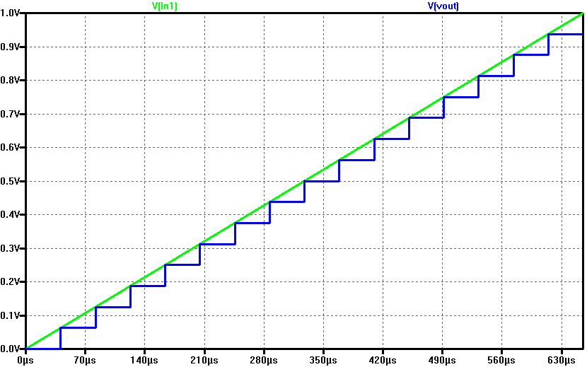
The graph on the right shows the input ramp voltage (in green) and the output step voltage (in blue). In total 16 steps can be seen which meets the expectation for a 4 Bit DAC. It is also possible to see by eye, that the step size is almost equal. For a more accurate analysis, an INL and DNL calculation is performed. |
|
INL & DNL of ramp signal
|
The graph below was generated by using the web tool Read LTSPICE raw data The stop time was set to 655.36 µs and the time step to 40.96 µs. This resulted in a total of 16 points, one for each voltage step. The voltage was then scaled to integer values (0 to 15). The INL and DNL values are not exactly zero, how we would expect from an ideal ADC and DAC, but int the +-micro range. This is due aproximation errors in LTSPICE. 
|
Histogram ramp signal test
|
For the histogram test the time step was changed to 5.12 µs. The extracted values were mapped to 15 integer numbers and the ADC histogram ramp analysis was performed. From the INL and DNL it is clear to see that the number of occurence is not equally distributed along the output, otherwise the error would be 0. 
|
Sine signal test
|
In this test a sine signal whith a frequency of 16784.66796875 Hz and a Vpp of 1 V is applied at the ADC input. The graph below shows the input voltage in green and the output voltage in blue. By eye it is difficult to see any deviation of the output signal, therefore INL, DNL and FFT analysis are performed. 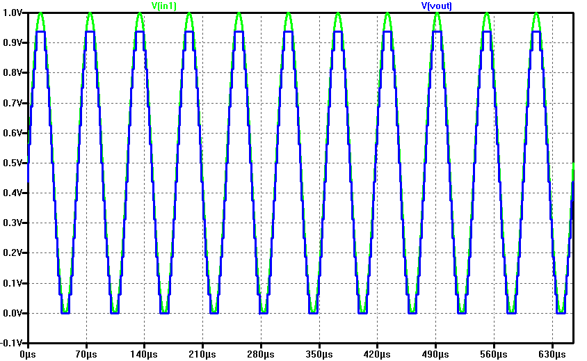
|
Sine signal INL & DNL
|
The graph below was also generated by using the web tool Read LTSPICE raw data The stop time was set to 655.36 µs and the time step to 5.12 µs. This resulted in a total of 128 measurment points. The extracted values were mapped to an integer number of 15 and the INL and DNL analysis was performed. The analysis shows that the output sine signal is not perfect. 
|
Sine signal FFT whith LTSPICE
|
Through LTSPICE it is possible to generate an FFT analysis. To do so, after having simulated the project, the FFT tool can be found under the option View and then FFT. Both input and output voltage are selected. From the FFT it is possible to see that the output voltage has a much heigher noise content. 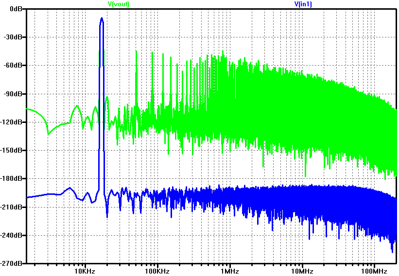
|
Sine signal FFT whith Web tool
|
An other FFT analysis can be done through the FFT Web tool In this case the result is less accurate because the FFT analysis was performed only on 128 measurement values. Despite this, a peak at frequency 11 can bee seen. The calculated SNR is 44,28 dB. 
|
R2R Ramp signal test
|
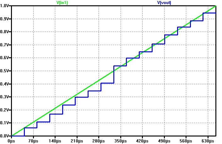
In this test a ramp voltage (in green) is applied at the input. The simulation time is 655.36 µs and the voltage range 0 V to 1 V. The DAC output voltage is shown in blue. At this point, whithout any special analysis tool, it can be seen that the single ouput voltage steps differ from each other. The biggest step happens when the MSB is flipped. |
|
R2R Ramp signal INL & DNL
|
Further investigation of the ramp signal through INL & DNL analysis shows that the transformation from digital to analog is not linear. Also the jump when transitioning from code 7 to 8 (flip of the MSB) introduces a significant error. 
|
R2R Sine signal INL & DNL
|
Whith the same sine signal of the previous tests an INL & DNL analysis was performed. When compared to the previous DAC it is possible to see that the error of the modified R2R DAC is higher, which meets our expectations. 
|
R2R Sine signal FFT whith LTSPICE
|
Through the LTSPICE FFT analysis it can be seen that the noise of the output voltage is higher than on the imput. But by eye no real differences to the previus DAC LTSPICE FFT can be seen. 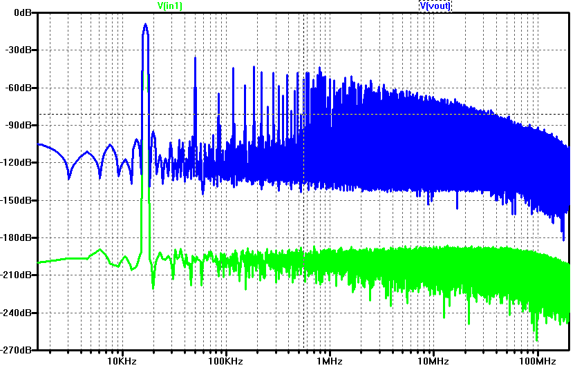
|
R2R Sine signal FFT whith web tool
|
Through the FFT web tool of Prof. Vollrath not only a grafics are displayed, but also signal magnitude and total noise magnitude in dB. From this values the SNR can be calculated. The results are shown in the table below. At frequency 11 the SNR is 23,18 dB, wich is much lower when compared to the 44,28 dB of the previous implemented DAC. This confirms tha the performance of the modified R2R DAC is lower. 
|