Teaching Advanced A/D Converters using Online Simulation and MeasurementsJörg Vollrath, University of Applied Science Kempten, Germany, Joerg.vollrath@hs-kempten.deAbstractThis paper is focused on teaching advanced A/D converters using theory, simulation and measurement. The successive approximation (SAR), sigma delta and pipeline ADCs were identified as the most common architectures [1] offering still some research challenges. Each architecture is taught using a textbook and theory, low level simulations with LTSPICE, high level interactive simulations with JavaScript, measurement of simple circuits and documentation with HTML pages. Therefore all material is open source and low cost. Interactive HTML pages allow to investigate different circuit topologies and ADC errors via high level simulation in the browser supporting deep learning. Modification in JavaScript source code gives more options to investigate state of the art A/D converters. Including measurements of resolution (ENOB), bandwidth, integral non linearity (INL), differential non linearity (DNL) and signal to noise ratio (SNR) in laboratory helps understanding limitations of theory and simulation. This approach was successfully applied in a master program of electrical engineering. Keywords-data converter, sigma delta ADC, pipeline ADC, laboratory, mixed signal design |
I. Introduction
Analog to digital converters (ADC) are important elements in electrical engineering incorporating high precision, high speed analog and digital circuits for control and error correction. Basic analog electronic circuits like low pass RC filters, amplifiers, sample and hold circuits and digital signal processing are applied. Complete material for data converter classes without laboratories can be found by Murmann [1], Khorramabadi[2], Baker [3] and Allen[4]. Another publication presented a data converter course with simulation, but no real measurements [5]. There are no courses available presenting analog circuit design, digital signal processing, digital error correction and measurement of data converters.
Simulations are valuable tools to understand theory by implementing equations and exploring variations. For circuit simulation SPICE variants (LTSPICE, PSPICE, Multisim) are used. Due to the large number of bits low level circuit simulation is very slow and requires a lot of memory and computing power. Therefore high level simulations are used to estimate data converter performance and understand conversion limitations. For high level simulation tools like MatLab Simulink or a programming language like C are used. These tools cost money and it is difficult to document simulation setup and results. This paper presents an approach using JavaScript and HTML for presenting low level simulations, perform high level simulations and complete documentation by creating interactive web pages [6].
Deep learning can be stimulated combining theory and simulation with realization, measurement and test [7]. Interactive tools like simulations give the students the opportunity to explore topics and deepen their understanding. Real measurements show signal and power supply noise and non idealities of circuits. The students learn how time consuming and costly measurement is. They see the gap between theory and real circuits. Therefore this paper also shows simple circuits realizations of ADCs to give the students the opportunity to study the gap between theory, simulation and measurement.
For data converter classes it is difficult to demonstrate challenges in circuit design. Real integrated digital to analog data converters (DAC) and ADCs show only hard to measure errors. On the other hand DAC architectures like a R2R converter can be easily built on a PCB board and performance and errors can be measured easily, if real components are used. Unfortunately DAC architectures are not using many challenging circuit concepts compared to ADCs. ADCs use sample and hold circuits, comparators and amplifiers with digital control and error correction blocks, which make them suitable for a laboratory.
The challenge is to select a simple ADC circuit, measurement equipment and build a low cost laboratory offering students opportunity to learn and explore mixed signal design.
There are also recent publications of sigma delta converters using simple passive RC circuits in combination with FPGA boards to show potential for low power ADCs [14,15,16]. This shows research potential for using discrete components to built ADCs and DACs. In the publications expensive signal generators and spectrum analyzers were used in conjunction with Matlab. This paper presents an approach for using low cost simulation with JavaScript and using self built DAC and ADC to measure performance lowering the total cost substantially.
The objective of this class is to provide complete in depth documentation of the covered topics. This should enable everybody to learn and understand operation of data converters, redo experiments and confirm theory. Emphasis is given to realize practical embodiments of ADCs in a minimum amount of time at low cost.
II. COURSE OUTLINE
The course interface electronics dealing with data converters in the master program electronic engineering is a lecture having sixteen 90 minute classroom presentations and thirteen 90 min laboratories. Basic topics are covered in the lecture before laboratories can start, leading to less laboratories than lectures. Since all used tools are free of charge and the laboratory is open during the week, the students can do additional work on the laboratories.
The 16 topics of the lectures are:(1) Introduction to data converters: N, Vref, Vfs, LSB, (2) LTSPICE simulation, (3) Static errors and measurement (INL, DNL, histogram), (4) Quantization error and spectral test, (5) DAC architectures: R string, charge scaling, interpolating, R2R, C2C (6) Errors in practical realization, (7) DAC practical considerations, (8) DAC implementation examples, (9) Analog to digital converte circuits, sample and hold (10) Dual slope ADC, Flash ADC and successive approximation ADC, (11) Basic building blocks of a pipeline ADC, (12) Challenges of a pipeline ADC, (13) Oversampling sigma delta ADC, (14) Advanced sigma delta architectures, (15) figure of merit and limits for ADCs, (16) summary and review of material.
Laboratory starts with 4 basic guided tasks: (1) Research State of the Art Literature, (2) Research latest commercia available AD and DA converters, (3) SPICE, DNL, INL, (4) Measuring a DA converter (INL, DNL, spectral test).
These laboratories are followed by an open laboratory covering the remaining time slots with varied tasks. Examples of the last years are: (1) Build and measure a discrete successive approximation (SAR) AD Converter, (2) Build a pipeline ADC and measure performance, (3) Create a 3-Bi digital to analog parallel charge scaling DA converter with LTSPICE, (4) Design and measure/simulate a sigma delta ADC, (5) Simulating a sample/track and hold for an analog digital converter and measuring the performance.
Simulations are done on circuit level using LTSPICE Documentation is done via HTML pages using JavaScript Special JavaScript modules allow embedding real LTSPICE drawings into HTML pages. The LTSPICE code for the circui drawing can be locally saved and LTSPICE simulation can be started locally. The students can use the simulation to confimr the statements in the documentation and do further explorations. The HTML page also provides FFT tools for signal processing and to calculate INL, DNL and SNR. So al schematics and simulations are publicly available to be able to redo simulations, confirm results, explore theory and design space.
Practical circuits are realized using cheap components on a bread board, a Nexys 3 FPGA board for data processing and having an electronic explorer board from Digilent fo measurement. Higher measurement accuracy could be gained using special commercial ADC, DAC boards, a high quality signal generator and a spectrum analyzer. This would also increase cost.
III. INTERACTIVE WEB PAGE FOR ADC ERROR SIMULATION
In literature the relationship between INL, DNL and spectral test is only briefly covered [x]. An interactive high level simulation web page [xx] was developed to be able to investigate.
The web page simulates a ramp and sine input signal for an ADC and calculates transfer function, histogram, spectrum with an FFT, signal level, noise level and displays results graphically (Figure 1).
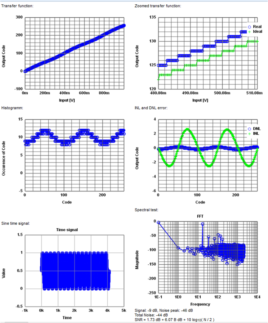
Fig. 1. Graphs for ADC input functions, INL ,DNL and SNR
4 ADC architectures, offset, gain, compare level, number of bits and errors can be selected (Figure 2). A flash ADC and 3 different pipeline ADCs are realized as a high level model with JavaScript. The code embedded in the HTML document for the pipeline ADC is shown here as an example:
for (var j = 0; j < nBits; j++)
{     // nBits pipeline stages
   if (input < cmp) {
     output = output * 2 + 0;
     input = addError(input) * gain + offset;
  } else {
    output = output * 2 + 1;
    input = (addError(input) - cmp) * gain + offset;
  }
  if (j ==0) { resx = input; }
}
For the number of bits (nBits) the input signal (input) is
compared to the compare level (cmp) and an output code
(output) and a residue as the new input signal is calculated
taking into account an Error (addError) a gain (gain) and an
offset (offset). These parameters can be entered at the web
page. For further investigations code can be modified or
extended. Figure 2 shows the user interface with the input fields controlling the simulation. All HTML elements can be used to create selection lists, check boxes and input fields. Equations can be included with a MathJS [17] module displaying graphically equations using LATEX style notations. easy to modify the appearance of the web page by using different style sheets or rearranging elements. This makes it possible to do all kinds of explorations and modifications to deepen understanding.
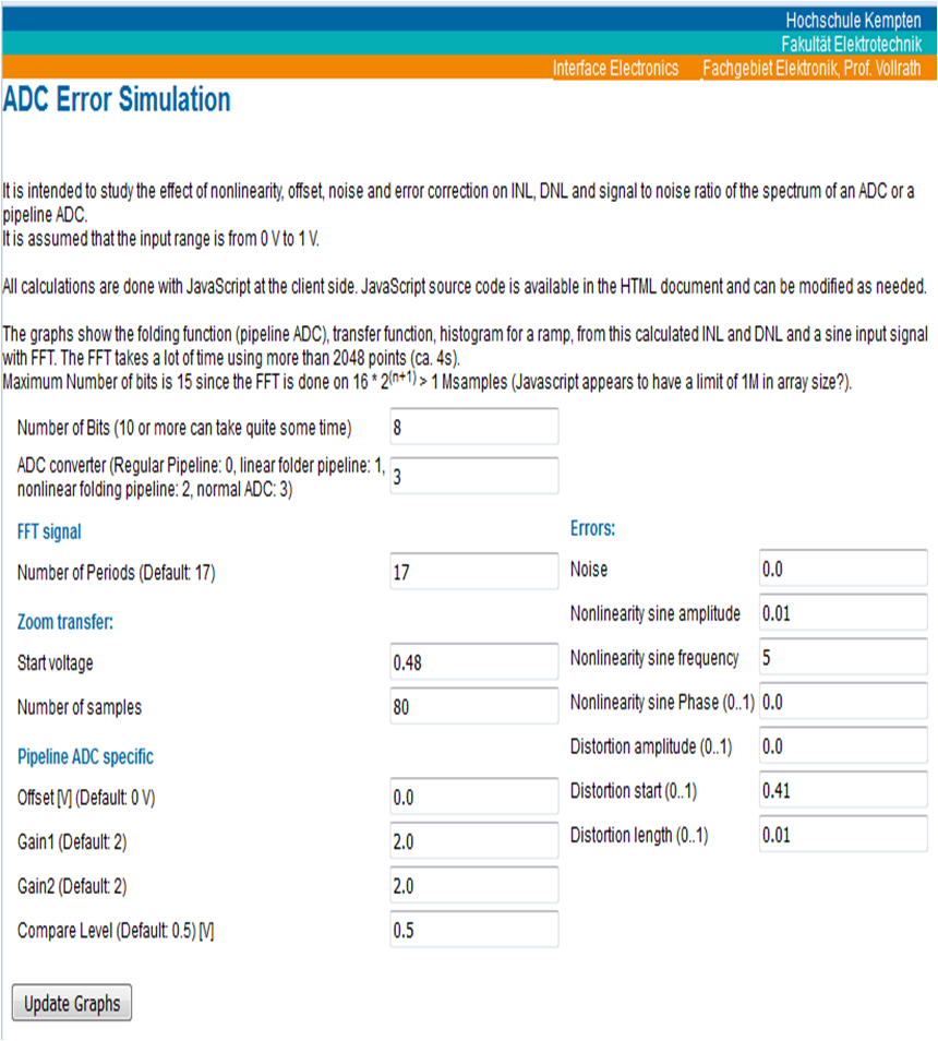
Fig. 2. Web page with input fields for ADC error simulation simulation
Many explorations can be done using this web page. Using 3 Bit resolution shows the textbook ideal transfer characteristic and can be modified using different errors. The signal to noise equation
SNR = 1.73 dB + 6.07 B dB + 10 log10(N/2)
B: number of bits
N: number of samples
can be confirmed varying the number of bits. Increasing the number of bits also increases program runtime to calculate the FFT and shows challenges of testing of high resolution ADCs.
Problems of estimation of SNR from spectral test results can be highlighted. Bleeding of the signal in the FFT can be shown using a non integer number of periods. Changes in SNR due to windowing can be shown. It is also shown how windowing is distributing the signal over more than 1 bin. Incomplete testing can be seen using a non prime number of periods.
Random and systematic errors can be added to the ADC to study the impact on transfer characteristic, INL, DNL and SNR. Adding a small sine function to the transfer characteristic gives higher order distortions in spectral test.
Also errors in linearity, offset and gain in a pipelined ADC can be introduced to study the effect on INL, DNL and SNR.
Since it is possible to pass information to a website via the link this page can be used during a lecture for displaying experiments. The starting values to show an effect of noise or systematic error are passed in the link and a good starting point of the simulation is initialized. Then the professor or student can start explorations. This was implemented in the accompanying slides to explain INL and DNL [13].
IV. ADC REALIZATIONS, EQUIPMENT AND MEASUREMENT
The successive approximation (SAR) ADC is a very robust easy to design ADC. It is widely used. Each block (sample and hold, comparator and DAC) can be optimized separately to optimize performance. Higher resolutions can be achieved with sigma delta ADCs and higher conversion rates can be implemented using pipeline ADC architectures. A sigma delta architecture provides digital signal processing challenges. A pipeline ADC needs matching of comparator, DAC and linear gain stage and presents an analog circuit design challenge. It is very difficult to optimize. All these implementations can be used to offer an open laboratory for students. To reduce circuit complexity very simple basic transistor circuits were used. Transistor models can be easily implemented in LTSPICE and can be fitted to real components. It is much more difficult to model integrated sample and hold circuits or operational amplifiers.
Low cost and ease of use of equipment is more important than high precision to enable widespread use in teaching. An Electronic Explorer Board is used as power supply, signal source and oscilloscope. A Nexys3 FPGA board is utilized for circuit control and data acquisition. The Nexys3 FPGA provides 3.3V levels and the logic levels of the Electronic Explorer board are 2.5V. To limit complexity and saving level shifters the ADCs work with 3.3V logic levels. The information is send via a serial interface to the PC for in depth data analysis. The FPGA can also generate control signals for a DAC to be used as a synchronized signal generator. The FPGA board with RAM can also be used to investigate error correction. Figure 3 shows a typical measurement system with error correction.
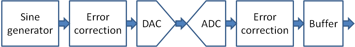
Fig. 3. DAC, ADC measurement system
A digital sine signal of sufficient accuracy has to be generated or stored in memory. For the DAC an error correction is needed for high resolution as a lookup table or a computation equation. This digital code can be fed to the DAC. The ADC needs also an error correction equation or lookup table (memory). Since it is difficult to perform a high quality FFT the measurement data are only stored in a buffer and then sent to the PC. Total cost of this system including measurement equipment is well below 1000$. Having limited measurement accuracy shows many real world test problems easily.
In case higher accuracy is required and more money is available commercial ADC and DAC evaluation boards can be connected to the FPGA and replace the Electronic Explorer.
All ADC realizations were presented to the students as an open laboratory using open questions. The students had to figure out how to measure and evaluate performance of the ADCs using the lecture material and online sources.
Since the different ADC architectures were used in different years, more and more features were added during this time frame. The first run of the class was done in 2010. In the first years only simulations for DACs and ADCs were done in the laboratory. In 2013 a pipeline ADC circuit was built on a breadboard and INL and DNL measurements and calculations were done. 2014 a charge coupling DAC was added. This was followed by a SAR circuit and a sigma delta circuit. In 2016 a tool was provided to automatically generate a sine function and then do a FFT and INL, DNL calculation on a web page. Since this shows the big effort required to develop a suitable master course laboratory, it was decided to publish the results for reuse. In the summary result table it can be seen how more and more measurement results could be done from one year to the next. The laboratory has reached a quality to make it worthwhile to reuse it.
V. SUCCESSIVE APPROXIMATION (SAR) ADC ARCHITECTURE
For the laboratory a list of parts, VHDL files for the FPGA and detailed assembly instructions are provided for the students. A R2R DAC is used and was built and measured in a preceding laboratory by the students [8].
The DAC provides many challenges. The first is to measure 1024 codes with sufficient accuracy. A digital volt multimeter can only be used with an automated measurement setup which was not available. An oscilloscope has normally only a resolution of 8 bit. Therefore averaging can be used to increase the resolution. Averaging K gives an increase in signal to noise ratio of
ΔSNR = 10 log K
leading to an increase of the effective number of bits (ENOB) of
\( \Delta ENOB = \frac{\Delta SNR}{6.02 dB}\)
Exact matching of the output voltage to the oscilloscope input range is also highlighted. Using a wide input range decreases the input sensitivity and the available resolution. This concept is also very important when ADCs are used for data acquisition in a real product.
Also overshoot and undershoot of the signal during the settling time of the DAC has to be excluded from averaging.
During LSB calculation students rounded the LSB not taking into account the resolution of the DAC. The LSB value has to have an accuracy of 1/2N. In the example the DAC has a range from 0V..3.3V with 10 bits.
\( LSB = \frac{V_{ref}}{2^{N}} = \frac{3.3 V}{1024} = 0.003222656\)
Rounding LSB to 0.00322 and using it for INL and DNL calculations resulted in systematically increasing or decreasing INL values.
The DAC spectrum was also tested. This topic is not highlighted in the available literature. It is assumed that only one sample is taken per generated code after the settling time. Students in laboratory often took more than one sample per code resulting in harmonic distortions and were not aware how critical synchronization between signal generation and sampling or filtering of the output is.
On the FPGA board for the SAR conversion rate, DAC operation and the number of bits can be controlled via switches on the FPGA board. The current ADC output code is displayed on a 4 Digit 7-segment display. The instructions can be found on the webpage [8]. Figure 4 shows the FPGA board on the left side with 2 USB connections for programming (top) and data transfer (bottom). PMOD connectors on the right right are used as input and outputs. An Electronic Explorer board on the right side provides the power supply, the arbitrary waveform generator and the oscilloscope. An R2R and C2C DAC circuit is built on the bread board part of the Electronic Explorer.
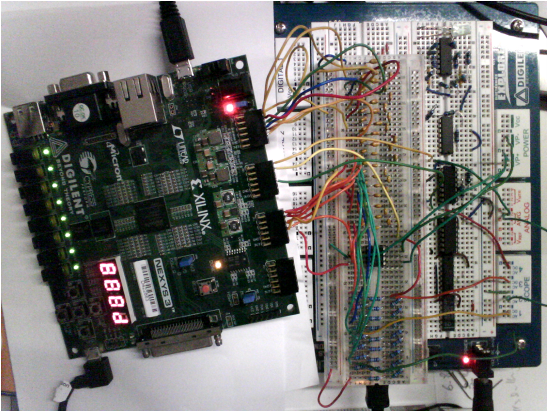
Fig. 4. SAR laboratory setup
The students first connected all parts and measured power supply, control signals and generated sine signal. They manually measured output voltage and SAR code for fixed voltage levels, before using a ramp and a sine signal and transferring data to the PC. On the PC they did data processing for the ramp signal to get INL and DNL. Finally they measured SNR of the sine signal.
The SAR ADC needs a stable input during the conversion time. This was realized with a sample and hold circuit. Students could measure the difference in INL, DNL and SNR with and without sample and hold circuit. The sample and hold circuit was also used to buffer the output signal from the passive DAC improving signal quality.
VI. FOLDING PIPELINE ADC ARCHITECTURE
Figure 5 shows a block diagram of a folding pipeline ADC.
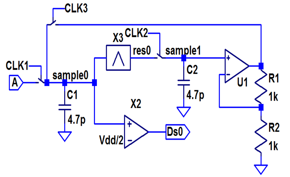
Fig. 5. A folding pipeline ADC block diagram
There is one input and three clock signals (CLK1, CLK2, CLK3). CLK1 transfers the input signal to the sample and hold circuit (sample0). The residue (res0) of the folder (X3) is sampled (CLK2), amplified and can be fed back to the input (sample0) via CLK3. This limits complexity of the circuit and allows serial operation of the pipeline ADC trading speed for resolution. The comparator is parallel to the folding stage taking out any speed limitations from the comparator. The residue is not depending on the comparator output making the ADC very fast. The comparator simply gives a 1-bit digital output.
The folding stage folds the input signal and amplifies it generating a residue with the same voltage range as the input signal. The residue is fed back to the input via switch CLK3 and generates the next bit of data. Therefore the sample rate and resolution can be adjusted with the clock signals and the number of stages. Building a single stage is sufficient to analyze the performance of the circuit. The resolution can be chosen by adjusting the number of times the residue is fed back to the input. Noise limits and calibration can be investigated. Each additional bit will need one more clock cycle reducing the sample rate. More stages can be used to achieve high resolution at high frequency.
Since the circuit should be used in a microelectronic centered class only PFETs and NFETs were used to realize the circuit on a PCB board. Figure 6 shows the LTSPICE schematic of the detailed circuit. Simulation statements and simple transistor models were included in this schematic. The documenting web page contains the LTSPICE drawing description, so a user can copy the LTSPICE code to a local folder and start simulating in LTSPICE right away. JavaScript takes care of showing the LTSPICE schematic on the web page. A level option controls how many details are shown.
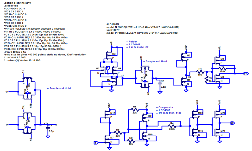
Figure 6: transistor level schematic of a folding pipeline ADC
The folding stage can be seen in the top center having an NFET (M5) and PFET (M6) in parallel and measuring the total current with a NFET (M4) at the bottom. The switch with CLK2 from figure 5 was moved between the folder and the gain stage to have a buffered sample and hold. The 2 inverter stages at the output are only used for simulation to get a good digital output signal. 9 NFETs and 9 PFETs are needed to realize this circuit. 2 ALD1106 and ALD1107 integrated circuits with 4 transistors each were used. 150k potentiometers were used to adjust gain and offset of the comparator and amplifier represented in the schematic by R1, R2, R3 and R4, R5, R8.
The same FPGA board as before is used in this laboratory. All VHDL code is included in the web site and detailed assembly and calibration instructions are given [9].
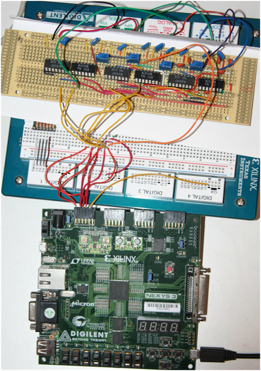
Figure 7: folding pipeline ADC laboratory setup
The real circuit shows the difficulty of calibrating the range and offset of the folding and amplifying stage. This gives emphasize to error correction using more than one bit per stage or using a lower gain. Measurements shows also other noise sources beside the quantization noise. Since this was one of the first laboratories, there was no buffer implemented on the FPGA board and only 38400 Baud communication was possible with the PC limiting the maximum input signal frequency and conversion rate. This highlights practical problems of data converters.
In this laboratory SPICE simulation can be compared to measurements. SPICE simulation takes a long time for a high number of bits and generates very large files. This motivates using high level simulators having shorter run times. The students experience the difficulties to handle a huge amount of simulation and measurement data. Measurements also give real data about nonlinearities and missing codes. Real data can also be used to investigate error correction. Differences between theory, simulation and measurement can be observed. Discharge and signal loss due to charge sharing in real sample and hold stages are also experienced during measurements.
VII. SIGMA DELTA ADC
A simple first order passive sigma delta ADC (figure 8) is covered in another web page [10] and laboratory. In the web page a high level JavaScript simulation of the internal voltage (INT) of the ADC over time using different R C values is used to demonstrate voltage swing limitations with the code shown before.
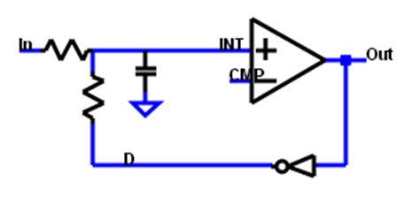
Figure 8: passive 1st order sigma delta ADC circuit
Filter type (sinc1, sinc2, sinc3) and oversampling can be selected to generate transfer curves and histograms. The students can explore the working of the sigma delta modulator with this simulation. Working VHDL code for the NEXYS 3 board is provided to realize these sinc filters in hardware. Finally a sine signal as input for the sigma delta modulator is used with different filters and windowing to display the output graphically and calculate signal to noise level. The bit width of the filter can be limited to demonstrate reduced signal to noise ratio. The signal to noise ratio can be changed using the different filters.
The web page was complemented by a real laboratory [11] in 2016. It uses the same components as the previous ADC architectures (Figure 9). Only R and C are added for the 1st order passive sigma delta ADC. A differential input of the FPGA is used as comparator. A reference voltage is supplied from the Electronic Explorer.
Measurements using an FPGA generated synchronized sine signal controlling a DAC showed challenges in matching the input range of the ADC to the output range of the DAC, covering all codes with no signal clipping. Some groups also experienced a flat middle part in the sine signal due to bad ground connection between FPGA, RC circuit and Electronic Explorer. These are practical problems showing up only during real measurement.
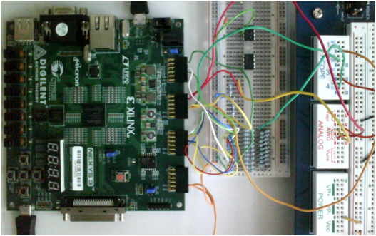
Fig. 9. A sigma delta ADC laboratory setup
A web page using JavaScript performs an FFT [12] of a input signal and calculates signal to noise margin taking into account the harmonics.
A typical measurement is shown in figure 10.
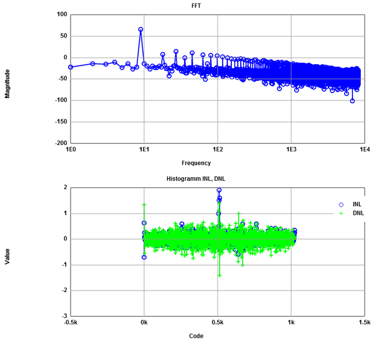
Fig. 10. FFT and INL, DNL from a sine signal
It became clear during the laboratory that it is difficult to calculate the signal to noise ratio. For the noise level the square root of all squares amplitudes are used without the signal amplitude
\( a_{noise}= 20 log \left( \sqrt{ \sum_{i=1, i!=i_{signal}}^{N_{FFT}} U_{i}^{2}} \right) \)
It is also interesting to remove harmonics from the noise and exclude it from the noise calculation. Therefore the program automatically orders the magnitudes and displays the signal level and the noise level. For each harmonic the power is removed from the total noise level, giving more insight into improvement potential. Table 1 shows in the first column the normalized frequency, the magnitude for the signal of this frequency and the remaining noise. In each line the power from the frequency contents above is removed from the total noise. This shows the potential accuracy of the ADC without harmonics.
Table 1: FFT analysis of a sigma delta measurement.
| Frequency | Signal magnitude dB | Total noise magnitude dB |
| 9 | 65.19 | 18.07 |
| 27 | 13.87 | 15.99 |
| 45 | 10.89 | 14.39 |
| 18 | 7.94 | 13.27 |
| 63 | 5.9 | 12.39 |
| 81 | 4.68 | 11.59 |
| 99 | 4.46 | 10.65 |
| 117 | 2.2 | 9.98 |
| 135 | -0.34 | 9.56 |
| 36 | -0.74 | 9.13 |
| 207 | -2.5 | 8.82 |
A signal to noise ratio of (65.19-18.07) dB = 47.12 dB giving ENOB = 7.5 can be seen. If the first 10 harmonics could be removed a SNR of 65.19 dB - 8.82 dB = 56.37 dB or ENOB = 9.07 can be achieved.
Only measurements showed a spread in the signal frequency when windowing was applied making the signal to noise calculation more difficult. Due to the measurement setup and equipment also high signal frequencies led to a spread of the signal to many bins around the signal frequency making signal to noise calculation difficult.
Using JavaScript for FFT and simulation saves the cost and teaching using a tool like MatLab, while still being able to analyze up to a couple of million points. The application runs on all platforms, even mobile smart phones with JavaScript enabled. It also offers a simple way to design a user friendly graphical interface using HTML and active buttons with JavaScript functionality. The run time of the JavaScript FFT application is still acceptable. At the same time INL and DNL is calculated from the histogram of the sine signal. This stresses the relationship between spectral test and histogram test. It makes it clear that for both tests a high number of samples (more than 2^B) are needed to guarantee correct operation and performance measurement of all codes. As an example 16k data points of a typical first order sigma delta ADC measurement are included and results are displayed.
During the laboratory the web page was updated due to the needs of the students. Since the webpage is accessed via the internet no distribution of a new version was needed, since there is only one version available at the web address.
VIII. SUMMARY
Simple, low cost ADC circuits and a measurement setups in all detail are presented giving a lot of opportunity for learning and research. It took 5 years part time work to achieve the present status. To enable faster research and learning this work is presented to a bigger community. The students feedback during the laboratory was very positive. They were a little surprised doing an open laboratory without detailed instructions, but were successful in doing the laboratory. Only open laboratories gave the opportunity to advance the laboratory setup.
This paper uses internet web pages to be open accessible. Providing open access detailed documentation makes experiments repeatable. The low cost of simulation using JavaScript, laboratory setup with Electronic Explorer and NEXYS3 board enables an easy access to learn about data converters. This is intended to improve the spread of knowledge.
Table 2 shows the current performance data of the investigated ADCs.
Table 2: ADC performance data
| ADC | sample rate [Samples per second] | Bandwidth [Hz] | Input range [V] | Signal to noise [dB] | ENOB |
| Pipeline | 500 | 11.9 | 0.7 .. 2.63 | -- | 7 |
| SAR | 6.1 k | 383 | 0 .. 3.3 | 36 | 5.71 |
| ΣΔ | 25M | 6.1k | 0 .. 3.3 | 47 | 8 |
All ADCs show typical challenges encountered when designing and measuring data converters. These challenges are not that easily experienced using typical evaluation boards for data converters. There is plenty room for improvement of the circuits to provide open laboratories in the future. Implementing calibration and error correction into FPGA is one goal. Improving manual calibration with modified potentiometer circuits or implementing a digital calibration for the pipeline ADC a second one. Investigations how to reach maximum speed and comparison to other ADC topologies is also interesting. A real test chip having superior performance would also help research.
The class is offered once a year. During the last 5 years each semester the available laboratory was improved due to the open laboratory type and new measurements of the students. Starting with a simple sigma delta converter having an averaging filter, a pipeline ADC with opamps and in another embodiment only with MOSFET transistors was explored. Next different DAC architectures were built and measured leading to a 10 bit R2R and C2C configuration. The DACs allowed to implement a successive approximation ADC and a sine waveform generator.
The FPGA provided at the beginning only control signals for the ADC and displayed results as thermometer code on LEDs. A 7-segment display was implemented next and some control switches to change sample rate, number of bits and filtering. Then a low speed serial interface was added to transfer data to the PC. A 16k buffer in the FPGA, a digital sinc2 filter and a digital sine signal generator allows at the moment higher resolution and higher speed measurements.
It is planned to make more options available via the serial interface and implement a larger buffer in the external RAM and increase the number of bits for sine signal. This allows measurements for high resolution ADCs. Error correction via lookup tables and digital filters in the FPGA is planned next.
REFERENCES
[1] Murmann, EE315B - Analog Digital Conversion Circuits https://web.stanford.edu/group/murmann_group/cgi-bin/mediawiki/index.php/Boris_Murmann
[2] Haideh Khorramabadi , EE247 Analog-Digital Interface Integrated Circuits, http://inst.eecs.berkeley.edu/~ee247/fa09/index.html
[3] Baker, ECE 615 CMOS Mixed-Signal IC Design, Spring 2009, http://www.cmosedu.com/jbaker/courses/ece615/s09/lec615.htm
[4] P. E. Allen, D.R. Holberg, CMOS Analog IC Design, http://www.aicdesign.org/scnotes10.html
[5] Quintans, C.; Colmenar, A.; Castro, M.; Moure, M.J.; Mandado, E., "A Methodology to Teach Advanced A/D Converters, Combining Digital Signal Processing and Microelectronics Perspectives," Education, IEEE Transactions on , vol.53, no.3, pp.471,483, Aug. 2010
[6] Vollrath, J., "Using models, simulation and measurements for teaching circuit design," Global Engineering Education Conference (EDUCON), 2013 IEEE , vol., no., pp.978,983, 13-15 March 2013
[7] J. Vollrath, "Interactive tools for teaching electrical engineering," 2014 IEEE Global Engineering Education Conference (EDUCON), Istanbul, 2014, pp. 129-133
[8] J. Vollrath, A real successive approximation ADC, https://personalpages.hs-kempten.de/~vollratj/InEl/SAR_ADC_real.html
[9] J. Vollrath, A real pipeline ADC, https://personalpages.hs-kempten.de/~vollratj/InEl/Pipeline_ADC_real.html
[10] J. Vollrath, Sigma delta ADC, https://personalpages.hs-kempten.de/~vollratj/InEl/SigmaDelta.html
[11] J. Vollrath, A real sigma delta ADC, https://personalpages.hs-kempten.de/~vollratj/InEl/SigmaDelta_ADC_real.html
[12] J. Vollrath, A JavaScript ADC FFT histogram application, https://personalpages.hs-kempten.de/~vollratj/InEl/FFT_Javascript_2016_Sigma.html
[13] J. Vollrath, Ideal ADC, INL and DNL, https://personalpages.hs-kempten.de/~vollratj/InEl/2016_10_10_03_InEl_DNL_INL.html
[14] Angsuman Roy, R. Jacob Baker, A Passive 2nd-Order Sigma-Delta Modulator for Low-Power Analog-to-Digital Conversion, 2014 IEEE 57th International Midwest Symposium on Circuits and Systems (MWSCAS)
[15] Fuyue Wang; Qiao Meng; Yong Liang m A 1.8V, 14.5mW 2nd order passive wideband sigma-delta modulator, Proceedings. 2005 International Conference on Communications, Circuits and Systems, 2005.
[16] Angsuman Roy; Matthew Meza; Joey Yurgelon; R. Jacob Baker, An FPGA based passive k-delta-1-sigma modulator, 2015 IEEE 58th International Midwest Symposium on Circuits and Systems (MWSCAS)
[17] MathJS, mathjs.org

| Dr. Ing. Joerg E. Vollrath received 1989 his Dipl. Ing. and 1994 his Ph. D. in electrical engineering, semiconductor technology at the University of Darmstadt, Germany. Since then he worked for the memory division of Siemens and Infineon Technologies and Qimonda in various locations in the USA and Germany. He is now a Professor for Electronics at the University of Applied Science, Kempten, Germany. His expertise and interest lies in the field of design of analog and digital circuits, programmable logic, test, characterization, yield, manufacturing and reliability. He has published 30 papers and has currently 32 patents. |