Online Data Converter FrameworkProf. Dr. Jörg Vollrath |


|
https://personalpages.hs-kempten.de/~vollratj/InEl/Vollrath_InEl.html
Hello everybody,
I want to present today an online data converter development framework. An online laboratory with electrical engineering background.
My name is Joerg Vollrath and i am professor at the university of applied science Kempten, Germany.
Lets look at the overview first.
I want to present today an online data converter development framework. An online laboratory with electrical engineering background.
My name is Joerg Vollrath and i am professor at the university of applied science Kempten, Germany.
Lets look at the overview first.
1. ADC Simulation
|
Error, Signal to noise ratio, INL, DNL, FFT Aliasing Bleeding Windowing DNL, INL Spectral analysis White noise Non linearity Single distortion Jitter |

|
First comes the ADC simulation of INL, DNL and spectrum analysis.
There is an interactive entry form, where an ADC architecture can be selected with a certain number of bits.
The simulation generates the transfer curve, INL and DNL error.
In this example it is zero since it is an ideal ADC.
Finally the spectral test is shown with the test signal and the noise.
Since it is very hard to estimate signal to noise ratio a table is summarizing these values.
As a real example a nonlinearity error is put in place with a sinusoidial function and an amplitude of 0.01.
An 8-bit ADC willl show some error. The graphs are updated. It takes some time in the browser.
The complete transfer function displays no visible error between ideal and real curve.
In the zoomed picture a big difference can be seen. The DNL shows little error,
but the INL shows the accumulated big error.
Comparing this with the FFT shows a harmonic signal because of the non linearity.
This tool can be used to look at errors, impact on INL, DNL and signal to noise margin.
Beside of noise errors, non linearity errors, distortion errors at a certain point in the transfer
function also jitter error can be simulated.
2.1. LTSPICE Simulation C2C DAC
Free easy download of schematic

The next laboratory is a LTSPICE simulation of a C2C DAC.
The LTSPICE schematic of the converter is presented on the webpage with all associated simulation code.
The displayed schematic is drawn on the web page from the used LTSPICE files.
A change in the LTSPICE will be reflected in the web page instantaneously.
The C2C structure can be seen and the ideal signal generator for the digital test signals.
There is a list with links to all needed files.
The user can download all necessary files for local simulation.
LTSPICE is a free circuit simulator.
2.2 LTSPICE Simulation Output File Analysis
with Calibration Possibility
|
Signal display FFT calculation in the browser INL, DNL calculation List of signal to noise ratio Calibration data |

|
The output data can be analyzed with a Javascript tool ReadRawFile_ADC.html.
This converts the output to positive integer data.
Then a FFT Javascript tool can be used to calculate the FFT.
Invoking the web page takes a while, since the web page starts with example sine data,
which is analyzed in real time during start.
The sine data are displayed, the FFT and the INL and DNL.
The user has a data input field to put in his data, choose the number of points, the number of bits,
the number of shown frequencies and windowing.
Hitting the buttons to read the data and process the data automatically updates the results.
The signal to noise ratio can be analyzed.
Additionally calibration is supported. Calibration data can be put into the input data field.
The ADC code and slope calibration compensates for the following data processing showing
potential improvement of calibration in signal to noise ratio.
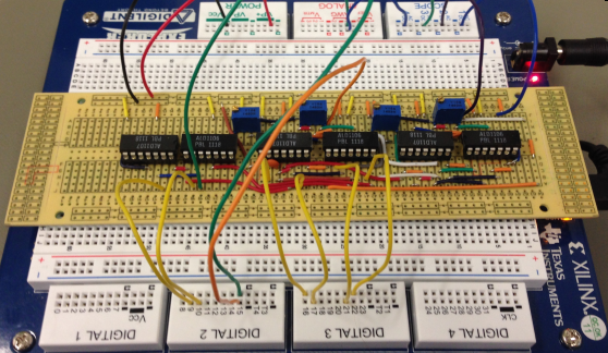
3. C2C DAC Circuit Realization and Measurement Instructions
|
Simple circuit Limited number of components Digital Signal generator Read oscilloscope data JavaScript ADC FFT |

|
The next thing is DAC measurement.
Here there is a laboratory, where the details to measure a C2C DAC is described.
There is a list of needed components.
The user needs an Electronic Explorer board to generate the digital input data and measure the output waveform.
There is also a schematic to build the circuit and a picture of the final measurement setup.
After building the circuit with the capacitances and the operational amplifier, there are
instructions how to measure the performance.
There is a video how to operate the electronic Explorer.
The same FFT analysis tools as before can be used.
Test signals can be generated with a DDS_Sim_Javascript and 2 files of digital patterns for a sine signals are provided. DDS_Sim_Javascript can generate integer numbers, EE vectors and VHDL vectors. VHDL code can be used for a FPGA to generate a digital pattern in real time at high frequencies. Parameters for signal generation are number of bits, number of periods, number of points and samples per points. DDS sine coefficients are also provided for a DDS generator. The generated signal will be analysed with FFT and signal and total noise is provided to verify the quality of the generated signal. This tool also supports calibration. Calibration values can be put in, which map the ideal digital sine value to the needed value for the real DAC. This shows possible improvements and potential of the DAC with calibration. The integer values, EE vectors or VHDL numbers are shown at the bottom and can be copied for further processing. The measurement oscilloscope data can be read with a web page Read oscilloscope data. After pasting the data, these are filtered according to start, step and averaging and total number of points.
4. ADC Simulation: 1st Order Passive Σ Δ ADC
|
Schematic Background signal and noise transfer function Signal simulation Digital filter: software and hardware High level simulation:
Signal to noise and ENOB 
|

|
The next laboratory is a ADC simulation of a first order passive sigma delta ADC.
A general schematic and a R, C schematic are shown on the web page.
There is a 1-bit ADC and a 1 bit DAC to feed back the data.
The web page explains the transfer function of this circuit, the bandwidth requirement and
then the high level simulation of the internal voltages and the
generated 0 and 1 data stream are presented.
For this simulation input voltage, timestep R,C factor and type of sigma delta converter can be selected.
Comparing an input signal of 0.8 V with an input signal of 0.6 V shows a change in the ratio of
'0's and '1's at the output and the different internal voltage around Vref/2.
The internal signal has a frequency relating to tones at the output data stream even if the input is only DC level.
Examples of bitstreams for different voltages are given.
SINC1, SINC2 and SINC3 digital filters are implemented with selectable oversampling rates as a simulation
on the page.
With a SINC1 filter and an oversampling rate of 4, 4 codes are generated.
This shows the potential of sigma delta converters of more bits and higher resolution.
The INL and DNL curves are also generated.
The physical implementation of the filter is presented. On the web page in the source code in JavaScript,
a schematic to build a circuit or as VHDL code, which can be downloaded for FPGA synthesis.
This makes it very easy for the user to built an ADC.
The spectrum can be analyzed.
Here a droop filter to compensate for low pass behaviour is presented.
There is a high level simulation for the spectrum combining the previous mentioned options.
Additionally the filter width can be chosen, the droop filter coefficient, the periods of the test signal
and the windowing.
To curves will be shown to be able to compare different settings of filter.
Displayed will be the input waveform and the output after the filter and then the FFT with a table
of signal to noise calculations.
Some results for simulations are also reported here. The user can look only at the results or
do his own simulation to confirm the results or investigate more.
One nice thing is that the simulator and the results and summary are displayed on the same web page.
Buttons can be used to hide or show sections enabling concise or extensive display of information.
5.1. Practical Realization AD
Successive Approximation Register ADC (SAR)
|
Complete Instructions Low Cost:
LTSPICE schematic available Data analysis online tools free: - Read data - FFT, INL, DNL, calibration |

|
Finally there are 3 different practical ADC measurements.
First is a successive approximation (SAR) ADC.
A cheap FPGA board, an Electronic Explorer and some electrical components are used.
5.2 Folding Pipeline ADC
 Very fast Analog circuit challenges High resolution Interesting for research |

|
Second there is a pipeline ADC presented with schematic, breadboard and FPGA control.
Instructions for calibration are given, how to get waveforms during conversion and typical data outputs. Typical improved transfer characteristic data are shown.
Instructions for calibration are given, how to get waveforms during conversion and typical data outputs. Typical improved transfer characteristic data are shown.
5.3 Laboratory Set Up:
1st order passive Sigma Delta Converter

Third there is a sigma delta ADC circuit with complete instructions.
The same FPGA board and Electronic Explorer is used.
A R2R DAC is used to generate the output waveform to synchronize input signal and ADC conversion.
Results are also presented with additional tasks for further investigations.
Outlook: Other Open Access Online Material
Elektronik 3, Digitaltechnik

|

|
This is an overview of all online laboratories.
Besides this laboratory there is also a laboratory for electronics covering diodes, transistors and
operational amplifers and a digital electronics laboratory going from a CMOS inverter to more complex logic
up to a finite state machine in a FPGA.
Thank you for your attention.
Thank you for your attention.