EE BenchJörg Vollrath, University of Applied Science Kempten, Germany, Joerg.vollrath@hs-kempten.deNewer document version: Research summary AbstractElectrical engineering needs a laboratory containing power supplies (logic, analog positive and negative, reference), arbitrary waveform generators, digital inputs and outputs, voltage and current measurements and an oscilloscope (4 channels). This equipment should be usable as semiconductor parameter analyzer (high accuracy measurement with curent and voltage limits), spectrum analyzer (high resolution ADC), digitzer (many channels with many samples), data logger (SD-card, battery supply) and sensor actuator interfaces (I2C, SPI, PMOD, Bluetooth). Measurement of electrical systems with IV curves, signal time behaviour and transfer functions (bode diagram) is one application. High accuracy, high speed and low noise measurements are required for data converters and need special measurement procedures. For prototypes serial transmission and receiving circuits, digital signal processing facilities and control blocks enable system development. A nice web user interface and no software installation would enhance the usability. This paper tries to develop such systems. |
Then the proposed system overview is given.
For the FPGA hardware the data acquisition, triangle, sine signal generator, UART and data buffer circuit description in VHDL is presented.
This specifies also the serial communication over the USB connector used by the nodejs server.
Next the user interface for AWG, oscilloscope, FFT and histogram was developed and is shown here for the hardware.
Finally a data converter characterization is done.
14.11.2023 How to Install Version V06
Version V06 Installation
Status 30.01.2023 Version V06
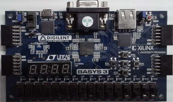
The Figure shows the BASYS3 FPGA board (150.- Euro) with 4 XADC channels at the left side and a 16 Bit 100k Ohm R2R DAC connectd to 2 PMODS on the right side. Next the configuration files for the FPGA and Node.js project can be downloaded. After installing Nodejs on a Windows PC this enables the web interface presented in the next figure to control an arbotrary waveform generator (AWG), an oscilloscope, a FFT and a histogram. A complete open electronics laboratory is therefore available. This documents tries to describe the open system and enable system extensions and modifications.
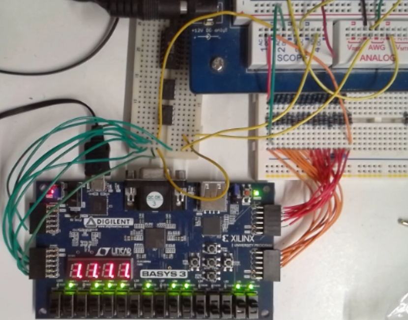
Figure: BASYS3 FPGA Board with R2R DAC and Electronic Explorer
VHDL project files EEBench_V06
Node.js project files NodeEEBench.bat as zip V06
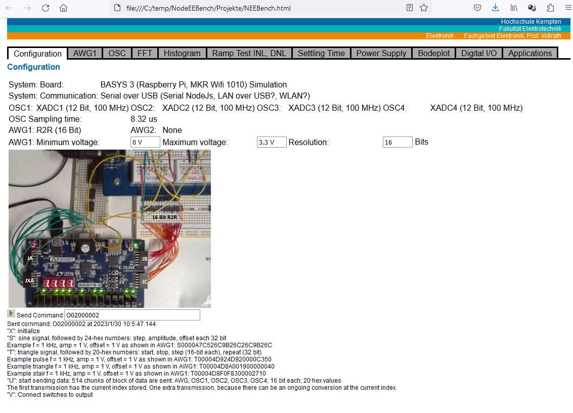
Figure: Nodejs, NEEBench user interface configuration page
Proposed system overview
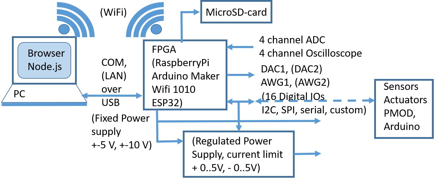
Figure: Propsed system overview
The figure shows the overview of the ideal proposed system. Functions in brackets are not implemented yet.
Features of BASYS 3 System and Software
- System: BASYS 3 with 230400 Baud serial interface over USB
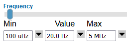
- AWG: 1 channel, 16 Bit R2R, 0..3.3V output range, 7.7 MHz sine
- OSC: 4 channel, XADC 1MSps (multiplexed x8) to 125 kHz, 0..1 V input range, up to 4k points
- The original digital code of AWG1 can be displayed as reference
- Variable buffer size is implemented
- FFT: up to 4k points signal and noise calculation, histogram display
- DAC characterization interface
- Switching between code display, voltage display
- Special trigger for ramp up test
Next steps
- 16 Bit R2R DAC characterization
- Power supply for positive and negative voltages for operational amplifiers to buffer the DAC AWG output.
- DAC characterization interface
- ADC upgrade: 24-Bit ADC, I2C, 16kSs, 6 channel MAX11259 PMOD 90.- expensive
- 2nd channel AWG: 16-Bit DAC, 1 channel, 100 kHz, SPI, MAX5216 23.-;
MCP4728 12-Bit DAC, 4 channel, 6us ca. 125 kHz, Command 3.4 MSps 15.- - AWG: White noise vector memory
- Bode plot
- Pipeline ADC with characterization interface
- Arduino Maker WiFi 1010
- PMOD DA2 ( 2 channel, 12-Bit, 125 kHz, 8 µs) 20.-
- PMOD AD2 ( AD7991 4, channel, I2C, 1 us conversion time, 12-bit ) 20.-
- Serial DAC
- ESP32
- RaspberryPi
- Simulator
- ZYNQ FPGA
- Test sequence control and interface
Use cases for this system
Applications can be an audio amplifier with microphone and speaker, filters, buck and boost converters, charge pumps, data converters, and motor control
An AWG1 generated signal (analog, digital IO) is measured with OSC1 and fed to an analog LCR filter circuit, or a SC-filter circuit (Digital switch control signals), or digital to a microprocessor and measured with OSC2 or (calculated digital signal).
The internal signal from OSC1 can be digitally processed internally and fed to AWG2 (analog and digital IO) and measured with OSC4 to compared it with the other solutions.
Static IV curve (Transistor, Diode, Opamp)
Bipolar transistor: UBE, IB (2 OSC channels), UCE, IC (2 OSC channels)
High current source with current limit IC
Low number of measurement points
Sine signal circuit analysis (amplifier, filter)
Positiv and negativ power supply (OpAmp), sine signal generator (AWG1), 4 channel signal measurement
Bode plot (Opamp, filter, LC meter)
Software control: AWG1, amplitude, frequency range, phase measurement
White noise generation and FFT
Signal processing
Digital FPGA logic or MACC blocks
Data converter characterization (offset, gain, INL, DNL, SNR, ENOB)
I. State of the art
Before this system was built available systems were reviewed:
 |
 |
 |
 |
 |
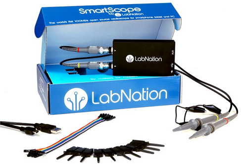 |
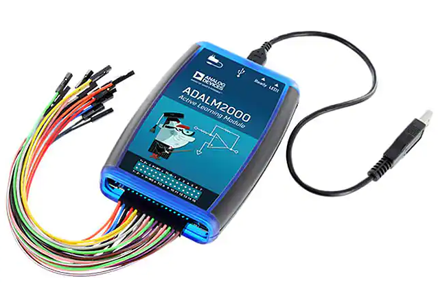
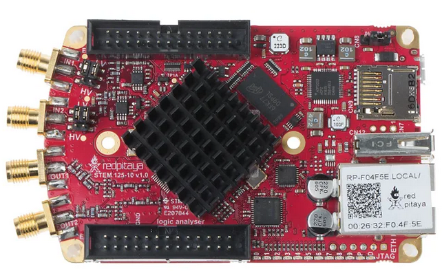
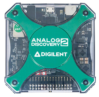
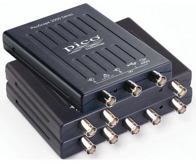
- Electronic Explorer (Digilent/National Instruments) (665 Euro, 2022, 350 Euro, 2010)
- ADALM2000 (Analog Devices) (300 Euro, 2022)
- Red Pitaya (250..450 Euro, 2022)
- Analog Discovery (450 Euro, 2022)
- PicoScope 2000 (100..1000 Euro, 2022)
- SmartScope (270 Euro, 2022)
The Electronic Explorer has a very nice user interface, which is of no cost and can be run in a demo mode without hardware.
The ADALM2000 is very cheap and has most of the functionality. It provdies a web server over USB connection, but needs a phyton install for software.
The Red Pitaya has a web interface and needs no software to be installed. Unfortunately also here a price-hike for higher precision was happened.
Most of the systems provide also a very detailed hardware description (schematic).
Example: Analog Discovery circuit description
A data converter code (not voltage) based control should be available.
The digital data of the AWG should be easily available.
There seems to be a trend to have only 2 oscilloscope channels and to increase the selling price for these systems.
Detailed tutorials to modify hardware and software are limited.
There seems to be room for a very cheap electronics laboratory.
This can be compared to the situation in the microprocessor realm where a very low cost Raspberry Pi Zero after the first generations of Raspberry pi is a huge success.
Basic and optimum system specification
Basic:
- 4 channel oscilloscope
- 2 arbitrary waveform generators
- Positive, negative, logic (3.3/2.5V) power supply
- 16 Digital IOs
- Breadboard with interface
- Web based user interface and simulation mode
- Digital IOs with digital interface (I2C, serial, SPI, gray code)
- Bode diagram
- IV curves: diode, transistor, opamp
- Data converter characterization with calibration
- Digital signal processing: filters, control elements, switched capacitor circuits
System overview
Software installation and updating is always difficult. The best solution would be, if the system is providing a WiFi or LAN connection via USB that can be operated via the browser.
The ADALM provides a LAN connection via USB, but there is no web interface available.
Most systems provide only a serial interface over USB. Therefore a nodejs application is built, which can be installed to provide a web interface and talks via the serial interface to the system.
A simulation mode should enable running the system without hardware.
Hardware solutions
A suitable low cost hardware was chosen for this project.
 BASYS3 |
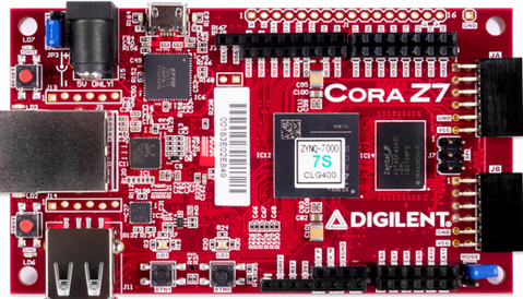 CORA Z7 |
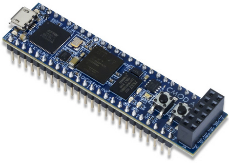 CMOD A7 |
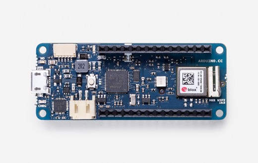
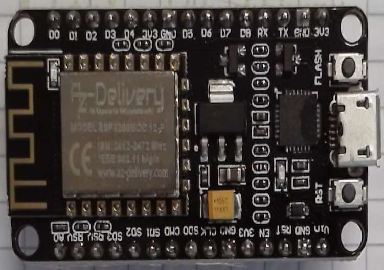
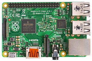 Raspberry Pi |
 MKR Wifi 1010 |
 ESP32 |
Figure: BASYS3, CORA Z7, CMOD A7, RaspberryPi, MKR Wifi 1010 and ESP32
The BASYS 3 board is used for the laboratory digital electronics. In this review ALTERA FPGA boards are still more expensive then Xilinix FPGA boards.
The MKR Wifi 1010 is used for laboratory Interface electronics. Raspberry Pis and ESP32 boards are used for various student projects.
Target:
- BASYS3 FPGA (140 Euro) (CMOD A7 (SRAM) 120.- Euro)
- CORA Z7 FPGA, uP(150 Euro)
- RaspberryPi (10.- - 100.- Euro)
- MKR Wifi 1010 (35.- Euro)
- ESP 32 (12.- Euro)
- NEXYS 3
- SAR ADC
- Sigma Delta ADC (7 Bit, 6.25 kSs, OSR 2048)
- Serial Pipeline ADC (7 (16) Bit, 10 Sps,
- R2R, C2C DAC
- C serial DAC
- MKR Wifi 1010
- 8 Bit, 300 Sps, R2R DAC
- 2 chan, 12-Bit, (125kHz) PMOD DA2 (20.-)
- 4 chan, 12-Bit, 1 MSps PMOD AD2 (20.-)
In the next section the developed VHDL code is presented.
FPGA Realization
Since VHDL code is more difficult than JavaScript client code as much calculation and verification as possible is put on the client side.
First the ADC implementation with the XADC is presented and then the arbitrary waveform generator for pulse, triangle, dc and sine signal.
Then the UART interface for control and data transfer is realized and commands are specified.
Extensive simulations of the circuits were done.
Finally a data buffer with control was realized.
XADC Wizard
The XADC can sample 4 differential channels on the BASYS3 board multiplexed.
Input range is 0..1V.
Sampling is done at 1 MSps multiplexing 4 channels.
Lower row JXADC is negative input, upper row positive input.
The FPGA has more XADC pins which can be used, but these are not carfully routed.
https://www.youtube.com/watch?v=2j4UHLYqBDI
- Basic:
- Interface Option: DRP
- Timing mode: Continous mode (always running)
- Startup Channel selection: Channel sequence
- DRP Timing options: 100MHz (Board frequency), 1000kS/s (maximum speed)
- ADC Setup
- Continous, Averaging None
- Alarms: unchecking not used
- Channel sequencer: choose channels
vaux6,7,14,15
Basys 3 FPGA xc7a35tcpg236-1
A file XADC_EE.xci is generated with the XADC interface.
my_adc : XADC_EE
  PORT MAP (
    di_in => "0000000000000000", -- input wire [15 : 0] di_in
    daddr_in => daddr_in,        -- input wire [6 : 0] daddr_in hex 16,17,1e,1f
    den_in => enable,            -- input wire den_in
    dwe_in => '0',               -- input wire dwe_in
    drdy_out => ready,           -- output wire drdy_out
    do_out => data,              -- output wire [15 : 0] do_out
    dclk_in => CLK,              -- input wire dclk_in
    reset_in => BTN(4),          -- input wire reset_in
    vp_in => vp_in,              -- input wire vp_in
    vn_in => vn_in,              -- input wire vn_in
    vauxp6 => JXA(0),            -- input wire vauxp6
    vauxn6 => JXA(4),            -- input wire vauxn6
    vauxp7 => JXA(2),            -- input wire vauxp7
    vauxn7 => JXA(6),            -- input wire vauxn7
    vauxp14 => JXA(1),           -- input wire vauxp14
    vauxn14 => JXA(5),           -- input wire vauxn14
    vauxp15 => JXA(3),           -- input wire vauxp15
    vauxn15 => JXA(7),           -- input wire vauxn15
    channel_out => channel_out,  -- output wire [4 : 0] channel_out
    eoc_out => enable,           -- output wire eoc_out
    alarm_out => alarm_out,      -- output wire alarm_out
    eos_out => eos_out,          -- output wire eos_out
    busy_out => busy_out         -- output wire busy_out
  );
The connector JXA is used for measurement and data gives a converted 16 bit value.
The channel is selected with daddr_in.Triangle generation
A triangle should accomodate excercising all codes of a data converter. Therefore start, stop and step values are needed. For very low frequencies or large periods a repeat parameter is used.
It has to be verified that start is lower than stop, that step is positive greater than 0. If the step size is not an integer times stop minus start the remainder has to be taken into account. If step is bigger than stop minus start a rectangle waveform is produced. Since VHDL code is more difficult than JavaScript client code as much calculation and verification is put on the client side.
The following relationship between FPGA frequency, signal frequency, resolution (number of bits), start, stop and step should be valid.
Input: fsignal, fFPGA, NBit, start, stop
For rectangle: step
output: (step), repeat
tri_unit: tri_counter
   port map(
      clk => CLK,
      reset => xrst,
      start => tstart, -- in std_logic_vector(15 downto 0);
      stop => tstop,   -- in std_logic_vector(15 downto 0);
      step => tstep ,  -- in std_logic_vector(15 downto 0);
      repeat=> trepeat,-- in std_logic_vector(31 downto 0);
      q => tout
   );
1. Calculation Rectangle:
The following variables are used for calculation.
Maximum Code of DAC: maxC, maximum voltage of DAC: maxV, AWG offset value: off, AWG amplitude value: amp
  var maxV = 3.3;
  var maxC = 32767;
  start = Math.trunc(maxC / maxV * (off-amp)); // start voltage to code
  stop = Math.trunc(maxC / maxV * (off+amp));  // stop voltage to code
  if (start < 0) start = 0;                     // no negative code
  if (stop > maxC) stop = maxC;                 // stop limited by maximum code
  step = stop - start;                          // adjust step to difference
  repeat = Math.trunc(1 / frequency / 2 * 1E8);    // 1E8 fFPGA
The 16-bit R2R 100k, 220k DAC needs 15 us settling time. The amplitude decreases above 30 kHz.
2. Calculation Triangle:
The code is the same for start and stop.
The difference is in the calculation of repeat and step.
  repeat = 1 / frequency / (stop-start) / 2 / 10E-9;    // 1E8 fFPGA
  if (repeat >= 16) {
     repeat = Math.trunc(repeat);
     step = 1;
  } else {
     step = Math.trunc(16 / repeat);
     stop = Math.trunc((stop-start)/step)*step + start;
	 repeat = 16;
  }
Due to the rounding the actual frequency is only
closely matching the required frequency.Table: Amplitude 3 V.
| Required frequency | 5 Hz | 50 Hz | 100 Hz | 200 Hz | 300 Hz | 500 Hz | 1 kHz | 10 kHz |
| Actual frequency | 5.22 Hz | 50.86 Hz | 98.7 Hz | 98.7 Hz | 197 Hz | 394 Hz | 888 Hz | 9.39 Hz |
3. Calculation Stair
A fixed number of 5 steps up and 5 steps down is implemented.
  repeat = Math.trunc(1 / frequency / 2 / 10E-9 / 5);    // 1E8 fFPGA
  step = Math.trunc((stop-start)/5);
  stop = Math.trunc((stop-start)/step)*step + start;
For a set of IV curves one generator can be programmed with a staircase and the other with a synchronized higher triangle frequency.
With the prepared list 1 kHz and 5 kHz or 2 kHz and 10 kHz can be used.
Sine generation
Research for realization of a sine generator in FPGA gives most of the time LUT solutions.
Values for sine are stored in a table and looked up. This is only feasable for small resolutions (up to 8 Bit).
LUTsize = NBit * 2
Table: Resolution and LUT table size
| Resolution (Bits) | 8 | 12 | 16 | 20 | 24 | 28 | 32 |
| Lookup table size (Bits) | 2k | 48k | 1M | 20M | 402M | 7.5G | 137G |
Calculation of sine can be iteratively done using complex calculations.
This can be used for iterative calculation with accumulated error or bitwise calculation for a certain value.
Iterative calculation minimizes computation effort between steps, bitwise calculation increases computation effort for each bit.
A combination of a limited LUT table 32..256 values or 5..8 bits and sine calculation would be an optimum solution.
Next value Re = (Current value Re * Step size Re - Current value Im * Step size Im)/2N
Next value Im = (Current value Re * Step size Im + Current value Im * Step size Re)/2N
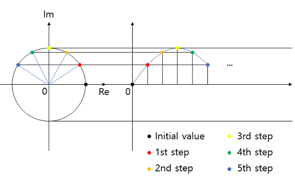
Figure 1: Example of complex number multiplication.
Challenges are:
- Signed large number multiplication in one clock cycle
- Rounding and Accuracy
- Transfer to a positive number (amplitude, offset)
- Calculating step size (Φ and complex numbers)
Verification of this procedure is done using FFT and looking at signal to noise ratio.
Since Xilinx DDS Sine Wizard gives up to 24 Bits resolution this realization targets 32 Bit.
- Precalculation of 32 to sine and cosine values for power of 2 fractions
sine(2 · π / 232 · 2i ) i=0..31 - Precalculation for a given frequency of step sine (Im) cosine (Re) by using for each bit the precalculated values
- Generating sine values
Applying the step to the current value
Accurate calculation for the next value 32*steps
sine_unit: sineX            -- Sine generator
   Port map (
       CLK => CLK,
       RST => xrst,
       step => step,            -- increment  in (31 downto 0) 32 bits
       amplitude=> amplitude,   -- signal amplitude in (31 downto 0) 32 bits
       offset => offset,        -- signal offset in (31 downto 0) 32 bits
       mysine => mysine         -- output waveform out (31 downto 0) 32 bits
   );
Sine Calculation example
fFPGA = 100 MHz
fsignal = 10 kHz
Number of points per cycle: Np = fFPGA/fsignal = 10000
step = 232 / Np = 429497
An FFT needs a power of 2 samples without windowing and an odd number of cycles to excercise as many levels of a data converter as possible
Choose NFFT:
NFFT (NBit) = 256 (8), 1024 (10), 16k (14), 1M (20), 16M (24), 1G (30)
Choose number of cycles:
Ncycle = 1, 11, 101, 1001, 100001
Calculate signal frequency:
Tsignal = NFFT / fFPGA / NCycle
fsignal = 1 / Tsignal = fFPGA * NCycle / NFFT
step = 232 / fFPGA * fsignal = 232 / fFPGA * fFPGA * Ncyle / NFFT = 232 * Ncyle / NFFT
NFFT = 1024
Ncycle = 17
fsignal = 100 MHz * 17 /1024 = 1.66 MHz
step = 71303168 = 04400000
| Number of cycles | frequency in kHz | Step |
| 3 | 1.40851 | 196608 = 3 * 64 * 1024 |
| 11 | 5.16452 | 720896 = 11 * 64 * 1024 |
| 101 | 47.419625 | 6619136 = 101 * 64 * 1024 |
+ Sine Simulation with JavaScript to verify VHDL
Oscilloscope
5 channel acquisition data are continously written into block memory. The current position and the number of samples is stored in position 2 and 3. These data are serially transmitted to the NodeJS server and then to the client (OSC).
The client sorts the data according to the bCount position (OSC1).
The trigger condition is searched in this data and data before and after the trigger point are extracted and displayed (OSC2).
Figure: Acquisition
Details can be found in "Data Acquisition"
UART
Since the received data is directly stored in signal generator registers there is no need for a FIFO.
Implemented commands (uart_mem.vhd, getCmd: process):
"X": initialize
"S": sine signal, followed by 24-hex numbers: step, amplitude, offset each 32 bit
"T": triangle signal, followed by 20-hex numbers: start, stop, step (16-bit each), repeat (32 bit)
"U": start sending data: 514 chunks of block of data are sent: AWG, OSC1, OSC2, OSC3, OSC4; 16 bit each; 20 hex values
The first transmission has the current index stored. One extra transmission, because there can be an ongoing conversion at the current index.
"V": Connect switches to output
"O": Oscilloscope block size 16 bit and sampling rate 16 Bit (V_06)
Command: O00200000 : Block size x0020 = 512; timeBase 0000 8.32 us
The mapping of uart_mem to block memory not registers is done starting EEBench_V04.
The multiplexer for sine, triangle switch is also done in EEBench using signal waveselect.
Baud rate 19200, 52us per bit, sine command: 25(chars)*10(Bit)*52us(bit time) = 12.5 ms
Baud rate 230400, 4.34 us per bit, sine command: 25(chars)*10(Bit)*4.3 us(bit time) = 1.1 ms
Baud rate 230400, 512 points 22 hex values each T = 0.5 s
+ EEBench V02
- EEBench V04
EEBench V04
The biggest change for V04 is the use of BlockRAM memory (myBuf) for data acquisition. After a "U" comman 514 x 5*4 Hex values are sent.
This is shown on the figure below.
Figure: FPGA blocks for EEBench
Simulation shows:
- Receiving of serial command RX, decoded with SEND trace
- triangle and sine at mywave.
- Data transmission to PC TX and bCount(memory address)
data always zero since no data stored before
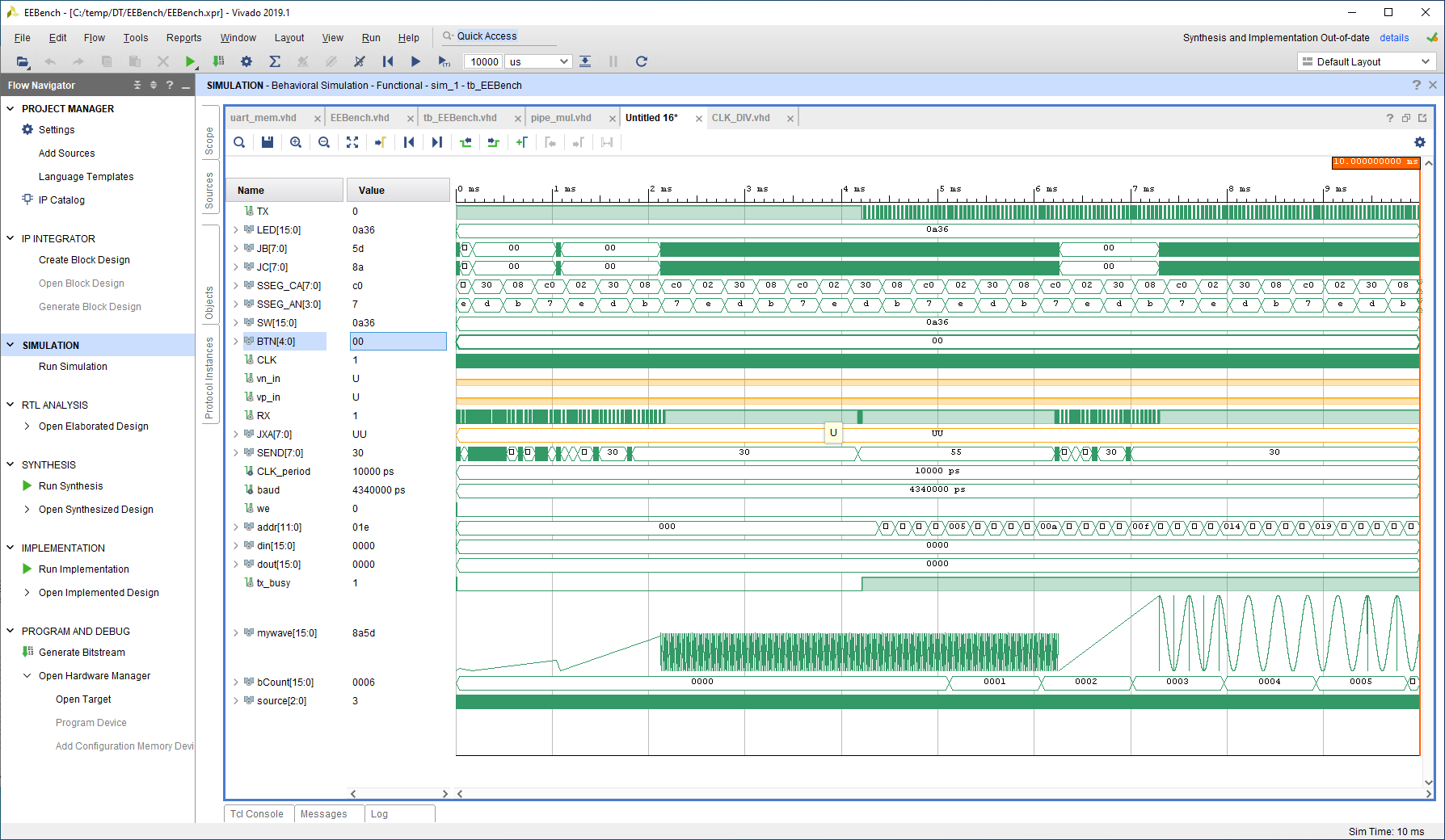
Figure: tb_EEBench.vhdl V04 simulation
Baud rate 230400, 4.34 us per bit, sine command: 25(chars)*10(Bit)*4.3 us(bit time) = 1.1 ms
+ Specification EEBench V05
EEBench V06
FPGA: Range of oscilloscope time base and buffer size should be extended.
Now the block RAM utilization is 2 out of 50 with 512 points. A factor of 16 8k points should be possible.
The transfer and sample block size should be user controlled.
So a UART command for change of sampling rate (16 Bit) and block size (16Bit) is implemented.
O<sampling><Block size>
Oxxxxxxxx
Update of NEEBench.js
Table: uart_mem: rxMem registers V06
| Input | memory address | Number of Bits | |
| rx_data_out | 0 | 8 | received command |
| a00000w1w0 | 8 | 8 | a '1' active '0' off w1w0: 01 sine, 10 triangle, 11 switches |
| Step | 16 | 32 | Sine step |
| amplitude | 48 | 32 | Sine amplitude |
| offset | 80 | 32 | Sine offset |
| (phase) | 112 | 32 | |
| (duty) | 144 | 32 | |
| tstart | 176 | 16 | triangle minimum start voltage |
| tstop | 192 | 16 | triangle maximum stop voltage |
| tstep | 208 | 16 | triangle voltage step |
| trepeat | 224 | 16 | number of samples per value |
| (phase) | 240 | 16 | |
| (duty) | 256 | 16 | |
| Block size | 272 | 16 | Oscilloscope block size (dataMax) |
| Time base | 288 | 16 | Oscilloscope time base (timeBase) |
- EEBench: rMem has already 512 Bits, initialization with 0 implemented
- uart_mem: UART receive set rMem: getCmd: process
when "01001111" => -- ASCII 49 O sine signal numD := "00001000"; -- 8 Hex numbers, (Step, amplitude, offset)x(8x4) rmAddress := to_unsigned(276,9); -- Start at index 276 (272 + 4) rx_mem(7 downto 0) <= rx_data_out; - Implement signals in EEBench:
dataMax for block size like variable NEEBench and timeBase
hook up rMem to dataMax and timeBase - For sampling a signal upSample is used
A process sampleRed is created to control sampling
-- sample rate reduction process --- time Base 000 upSample always 1 -- timebase 001 upSample 1-16-times-0-16-times -- timebase 010 upSample 1-16-times-0-32-times sampleRed: process(CLK, BTN(4), readyX) variable jCnt: integer; -- counter for reduction variable kCnt: integer; -- 16 samples begin if ( BTN(4) = '1') then -- asynchron reset with button 0 jCnt := 0; kCnt := 0; elsif (rising_edge(CLK) and (readyX = '1')) then kCnt := kCnt + 1; if (kCnt >= 8) then -- Clk divider 8 by kCnt kCnt := 0; jCnt := jCnt + 1; if (jCnt >= timeBase) then -- upSample short '1' long '0' upSample <= '1'; jCnt := 0; else upSample <= '0'; end if; end if; end if; end process; - TimeBase in NEEBench.html
- Introduce global variable timeBase
- Connect a serial command to change time base
timeBase > 200us/div timeBase = 1
timeBase = timePerDiv / 200E-6
timePerDiv is text input: id="baseVal" with unit value
Update of FPGA with 'Run' command and change in field (functions readCRX,comboBox)
Create function updateOSC for comboBox and readCRX
In updateOSC creat cmdO ="O00200000"; Block size x0020 = 512; timeBase 0 8.32 us
function confOsc() {
          var cmdO = "O";
		  // alert(document.getElementById("dataMax").value);
		  dataMax = parseInt(document.getElementById("dataMax").value); // 512: 0200
		  cmdO += decToHex(dataMax,4);           // Block size first
		  timeBase = Math.round(unitToValue(document.getElementById("baseVal").value)/200E-6);
		  cmdO += decToHex((timeBase + 1),4);   // Sampling next FPGA 0 and 1 same!
		  // update command field
		  document.getElementById("cmdTxt").value = cmdO;
		  sendCmdC();                           // send OSC configuration
}

window.addEventListener("load",confOsc());

function updateOSC(){
	   // update value field
       updateChanFields();
	   updatePlot();
       confOsc();
}
Attention interaction change during data acquistion? Probably not, only one bad display
Adjusted var timestep in function socket.on('newData', function (data) {
- Verification of timeBase FPGA code and NEEBench.html
Compilation FPGA, html and js correct during loading
Operation: timeBase 0,1 give same maximum sample rate for FPGA -> fix NEEBench
Operation: 2 ms/div x axis not fully filled? Sample rate too high time Base too low fixed with the following code
timeBase = Math.round(unitToValue(document.getElementById("baseVal").value)/200E-6); cmdO += decToHex((timeBase + 1),4) // Sampling FPGA 0 and 1 sre the same - Block size NEEBench: already global variable dataMax present
Tab configuration field 'Sampling memory size' with selection 1,2,4,8,16,512,1024,2048,4096,8182
Read field before sending command
Use field value during receiving data
var timeSampling = unitToValue(document.getElementById("timeSampling").value); var timestep = timeSampling * (timeBase + 1); // XADC 10ns * 8 * 104 cycles conversion - Block size FPGA EEBench
- Increase memory size of structure:
one_port_ram.vhdl defines blockRAM
Instance: myBuf: One_port_ram with signal addr (addrUART, addrGen)
uart_mem aBuf, tma, tmAddress - Increase acquistion
- Increase uart transfer FPGA, ServerEEBench.js, NEEBench.js
- Debugging of block size and sample rate with AWG as reference and FFT gave 96 dB equivalent to ENOB = 16 Bit
- Open: Challenge of acquisition for large Blocks and large sample times
- At the moment AWG and ADC data is stored all the time in memory.
When a data request is received sampling stops and the data is transfered
as block to the client. This takes 0.5s for 512 data and current baud rate.
The client waits until all block data is received
and updates the chart.
During Run operation every 1 second an Intervall function tries to get new data.
For large blocks or large acquisition times update is very slow.
Solution: There should be a plot every n received data?!
Solution: Large times should have small block sizes and acquisition continues?
- Open:
When to switch from block transfer to individual transfer?
Should the block size be automatically adjusted?
Update setInterval adjustment?
User interface
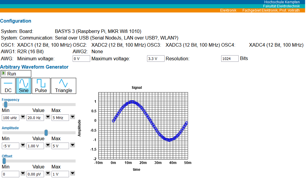
+ Arbitrary Waveform Generator
- NodeJS
Starting point is copying of the HTML and Javascript sources to C:\temp\NodeEEBench
The following files are important:
NodeEEBench.bat this starts ServerEEBench.js
ServerEEBench.js the nodeJS server file
In the subdirectory Projekte the file Signalgenerator_221111.html is located.
An example of nodeJS communication is done in Webeditor.
The latest version of serial port on windows requires the following commands:
   var SerialPort = require('serialport').SerialPort;

   SerialPort.list().then(  // List available serial ports
       ports => ports.forEach(console.log),
       err => console.error(err)
    );

    var serialPort = new SerialPort({
      path: "COM22",        // port name
	  baudRate: 230400      // Baud rate befor 19200, 52 us per bit
    });
The io.on subroutine detects user connection and logs it on the console.Then the socket event of a cmd from the client is implemented.
The most important feature is to detect the block size for sending data.
The serialPort.on 'data' subroutine collects data from the serial port and emits it to the client.
    io.on('connection', function(socket){
		var con = true;                             // connection still valid?
        console.log('An user is connected')

        // get data from connected device via serial port
		var dataBuf="";

         socket.on('cmd', function(data){     // get client event
        	var cmdName = data.value;        // cmd passed from client
        	console.log('cmd: ' + cmdName);
			if (cmdName[0] == "X"){
               dataBuf = "";
			}
    	    if (cmdName[0] == "O"){   // oscilloscope block size next 4 hex values
               dataMax = hexToDec(cmdName.substring(1,5));
			   console.log('Block size: ' + dataMax + "x" + cmdName.substring(1,5) + "x");
			}
    	    serialPort.write(cmdName);           // hex(cmdName)
			// insert server action commands
			// var data= "Test Data:" + cmdName;
    		// socket.emit('newData',{value: data });  // send data to client
        });

	    serialPort.on('data',
		  function (data) {
		    // get buffered data and parse it to an utf-8 string
			var data1 = data.toString('utf-8');
			dataBuf += data1;
			// you could for example, send this data now to the the client via socket.io
			// io.emit('emit_data', data);
			if ((dataBuf.length >= 22 * dataMax ) && (con)) {   // complete set
			 console.log(dataBuf.length/22 + "," + dataBuf.length + "," + dataBuf.substring(0,50));     // dataBuf
		     socket.emit('newData',{value: dataBuf});  // send data to client
			 dataBuf = "";
			};
 		 } );

        socket.on('disconnect', function(data){
    	    console.log('An user is disconnected');
			con = false;
        });
    });
+ Oscilloscope
Oscilloscope User interface
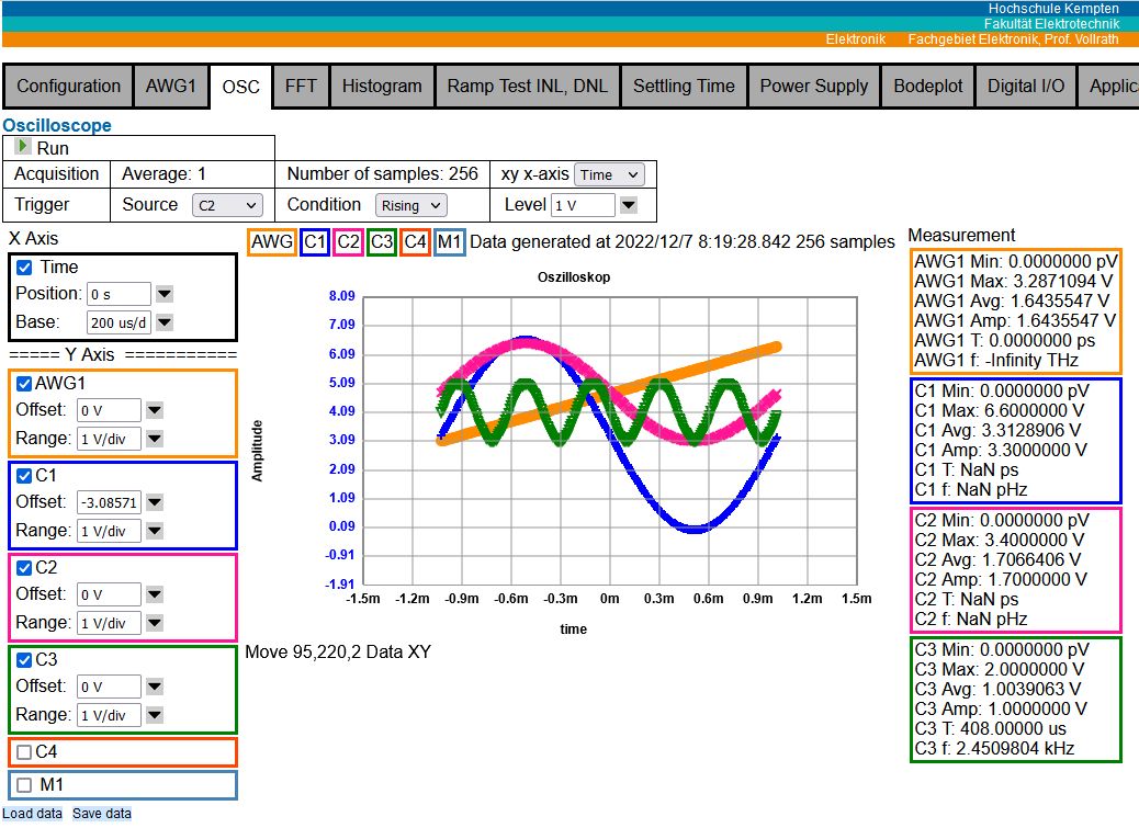
Figure: Oscilloscope interface V05
The figure shows the oscilloscope interface with the run button at the top.
Acquisition options are shown with xy-axis selection operational for version 5.
A trigger source, condition and level can be chosen.
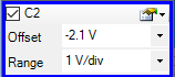
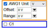
On the left are the axis control with offset (position) and range (base).
Below are 2 buttons to load example data and look at the data with save.
The curves are color coded displayed and typica measurement values are displayed at right column.
Cursors and math functions are still missing.
+ ComboBox
Run Button
The icon changes from run to stop.Run emits a serial "U" command from client to server (function oOp('Run')) and starts a (handlerOsc = setInterval(runOsc,1000);) continues sampling every second. busyOsc = 1; and oState = "Run"; is set
Stop emits ..(function oOp('Stop')) and sets oState = "Stop";
Acquisition
Version 5:A block of 512 data points is acquired and searched for a trigger point and 256 data points are selected for display.
5 16 bit values as 4 hex digits each are sent with a start and stop character.
Here is an example for 2 samples 5 channels each.
U4710FF0F471000000000YX0000000000000000D119Y
A new block starts with an "U" and each data value is limited by an X and Y.
Trigger
Trigger implementation
Measurements
Measurement data are generated with function chanStats().
For each channel the data points are searched for minimum and maximum and average is calulated.
     var min = dataOSC2[i*dataMax/2];
     var max = min;
	 var avg = min;
     for (var i1 = 1; i1 < dataMax/2; i1++) {
       var point = dataOSC2[i*dataMax/2 + i1];
	   if ( point < min) min = point;
	   if ( point > max) max = point;
	   avg = avg + point;
     }
	 channels[i].min = min;
	 channels[i].max = max;
 	 avg = avg/dataMax*2;
	 channels[i].average = avg;
     channels[i].amplitude = (max - min)/2;
Everything is stored in the object array channels.Average value is used for period and frequency.
Each crossing of the average value of the curve is collected.
	 // period and frequency
	 var t = new Array;
	 for (var i1 = 1; i1 < dataMax/2; i1++) {
       var point1 = dataOSC2[i*dataMax/2 + i1];
	   var point2 = dataOSC2[i*dataMax/2 + i1 - 1];
	   var point3 = point1;
	   if (point1 > point2) { point1 = point2; point2 = point3; }
       if ((point1 <= avg) && (point2 >= avg)) {
	      t.push(i1);
       }
     }
Finally the differnece between 2 crossings and the average of these numbers is used for frequency and period.
	 // Differences between t(i) half period
	 var tx = new Array;
	 for (var i1 = 1; i1 < t.length; i1++) {
	    tx.push(t[i1]-t[i1-1]);
	 }
	 var periodAvg = 0;
	 for (var i1 = 1; i1 < tx.length; i1++) {
	    periodAvg += (t[i1]-t[i1-1]);
	 }
	 periodAvg = periodAvg / (tx.length-1) * (dataOSC2[1] - dataOSC2[0]) * 2;
	 channels[i].period = periodAvg;
	 channels[i].frequency = 1/periodAvg;
The displayed values can be easily selected and copied.FFT
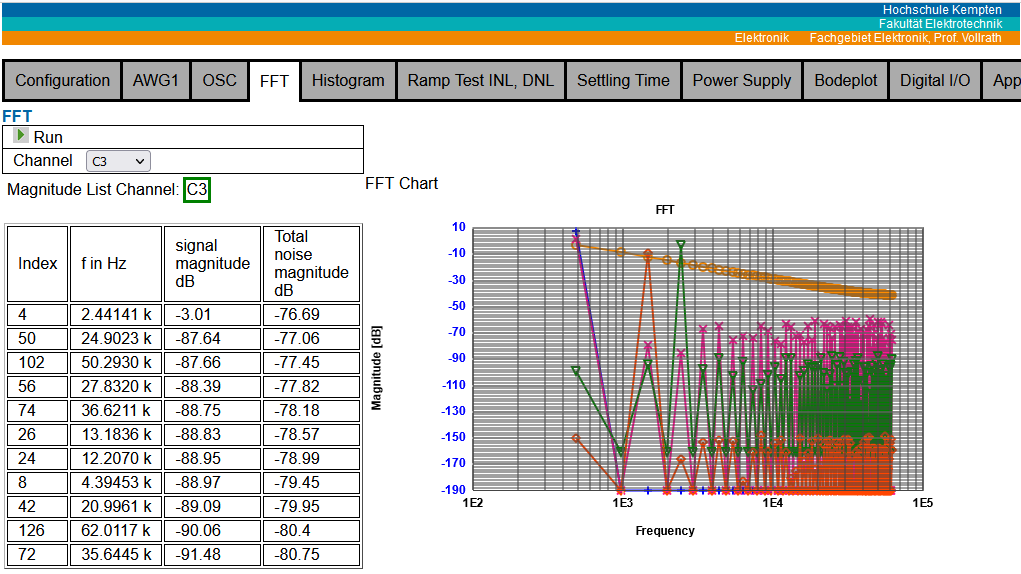
Figure: FFT interface V05
The figure shows the user interface for the FFT. The Run button activates and runs the FFT once. 256 data points at 8.32 us acquisition give a minimum frequency of 4.6 Hz and a maximum frequency of 60 kHz.
Data was generated internally with the function generateData().
The y values of the channels were scaled by C2 256 (8*6 = 48 dB), C3 4096 (12*6 = 72) and C4 2M (21*6 = 126 dB).
For C3 the largest peaks are listed (choose via channel select list).
For C3 at 2.4 kHz the signal has -3.01 dB and total noise is -76.7 dB as expected.
C1 has 280 dB signal noise ratio equivalent to 280/6 = 46 Bits.
The y axis has a fixed range implemented.
Ideal sine curve calculation can give more than 32 bits -192 dB.
Typical user cases have to be investigated to improve the y-scaling.
Details can be found in FFT Implementation
Histogram
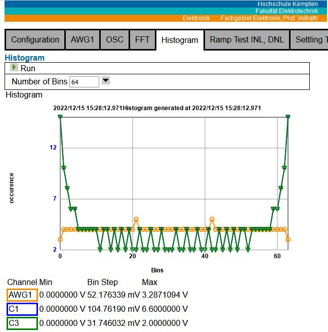
Figure: Histogram interface V06
- Run button (function hOp(cmd))
- Combo box number of bins (var nBin)
- Function generate histogram (var histo = new Array();)
- Chart: canvas id="histoChart"
Settling time (Pulse)
INL, DNL (triangle)
SNR (sine)
Calibration
User circuits
A simple RC circuit.
AWG1 signal is externally applied to an RCL circuit and the output voltage is measured with OSC.
Instead of an RC circuit a switched capacitor Cswitch,CL circuit can be used. The switches should be digitally controlled. Cswitch should match the R and the output should match the first result.
Cswitch = 1/R/fPGA
Third option would be a digitally processed digital AWG1 signal which is displayed after signal processing in the OSC window or fed to AWG2 for output and can be measured with OSC.
Voutn+1 = Voutn + (Vinn-Voutn)/R/fCLK/C
Voutn+1 = (Vinn + Voutn * ( R * fCLK *C - 1)) * 1/R/fCLK/C
How does the schematic symbol look like?.
These 3 design options can be compared.
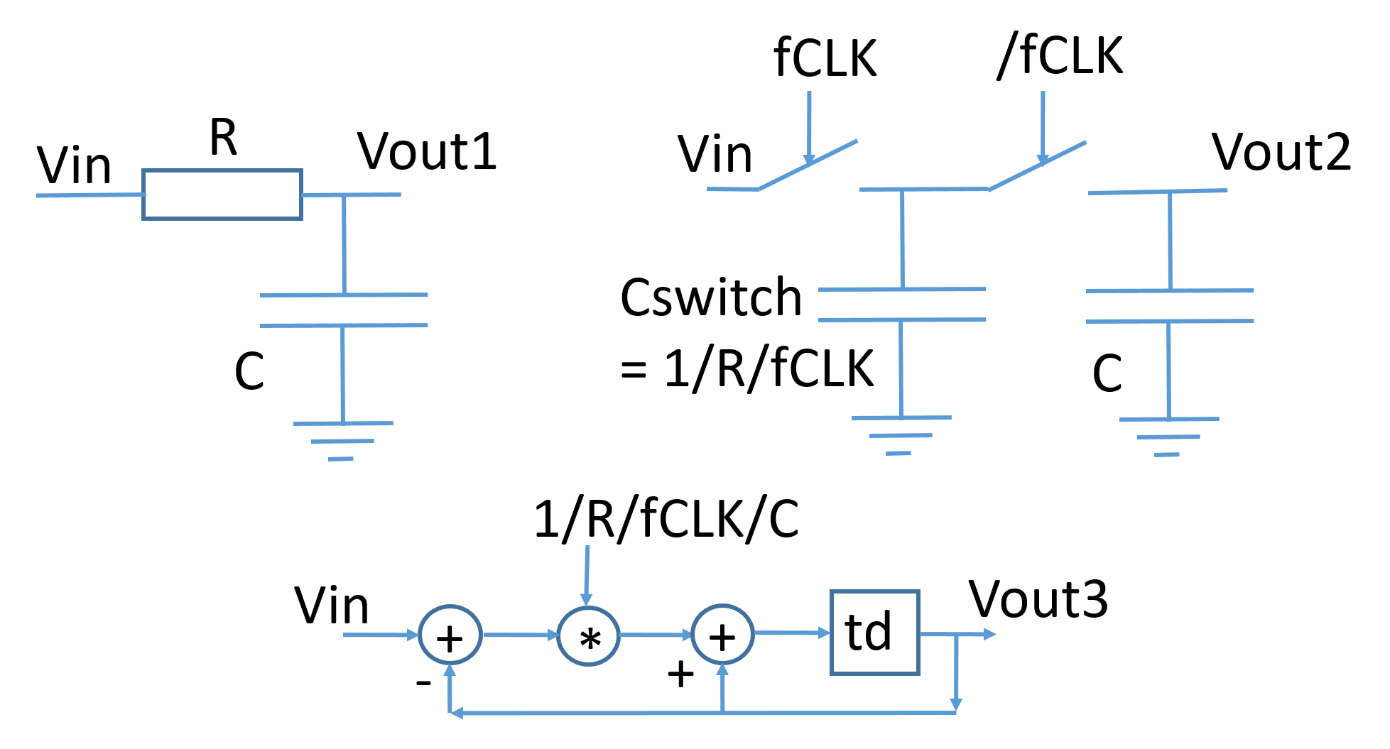
Figure: RC Circuit realizations (td=1/fCLK)
A DAC/ADC error correction
The internal digital sine signal is fed to a lookup table or equation and then diplayed (OSC) and passed to the external DAC under test.
The OSC input signal is digitally processed via equation or lookup table and the resulting signal displayed or processed for DNL, INL and SNR.
Filters, control loops, ...
Paralell, seriell conversion
Taking the AWG sine code and converting it to a serial DAC code.
Taking serial gray code output of a pipeline ADC and converting it to binary numbers.
+ More Hardware
+ Proposal for EEBench hardware
Data Converter GUI
Texas Instruments
Texas Instruments, High Speed Data Converter Pro GUI, User's Guide, SLW087D, march 2017
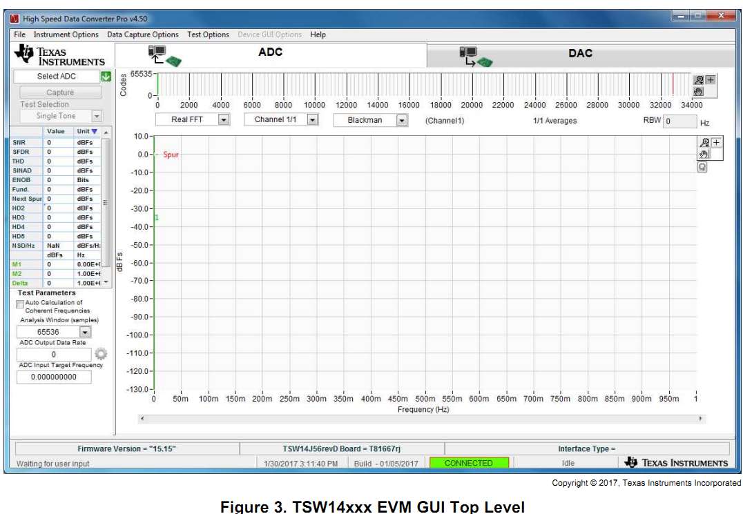
Figure: TI GUI Top level ADC
Select ADC or DAC, Small time window, large FFT window, windowing, code display, SNR, SFDR, THD, SINAD, ENOB, Fund., Next spurios, HD2, HD3, HD4, HD5
Samples, output data rate, input target frequency
2 channel display
Eye diagram, channel power measurement
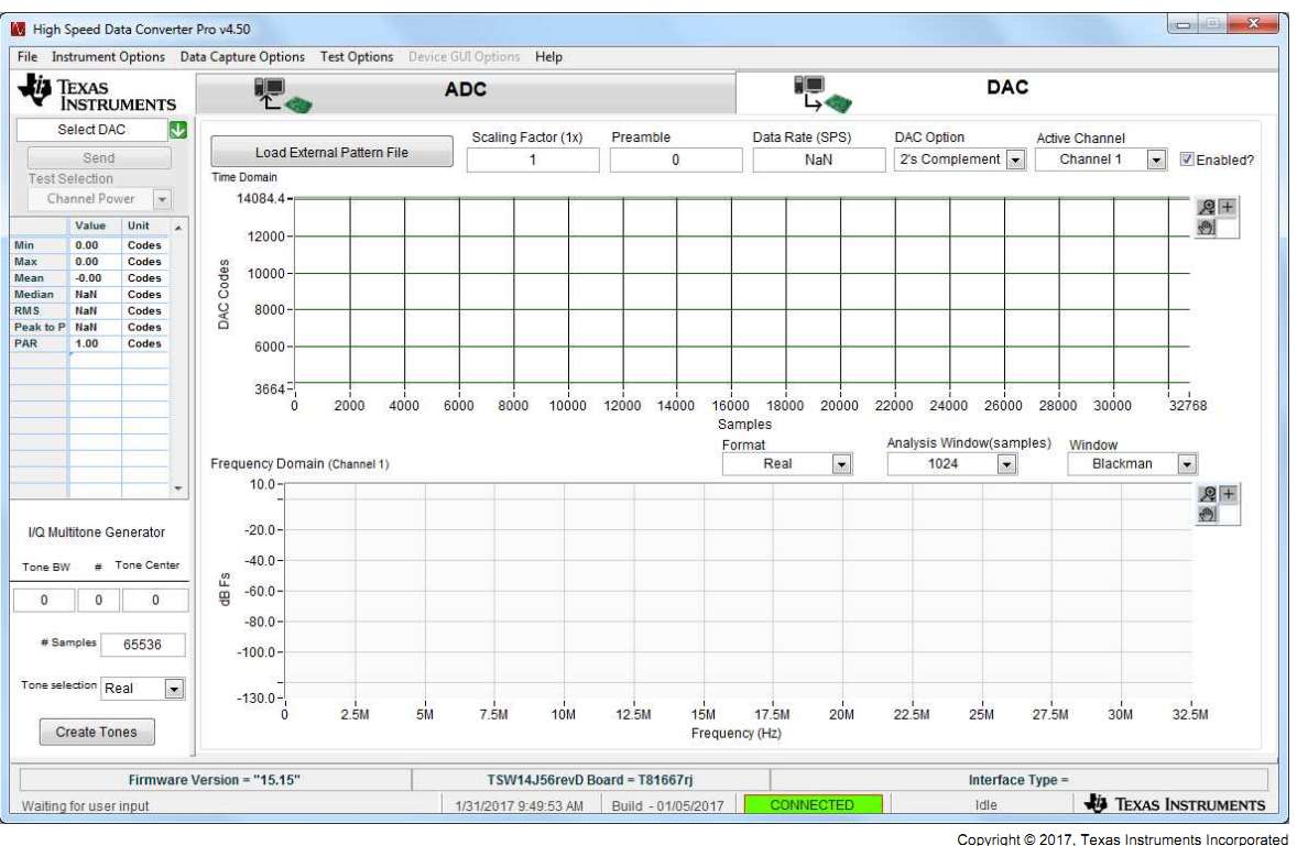
Figure: TI GUI Top level DAC
DAC vector file 16-bit, 16k or 4096..512M vectors
Multitone generator
Example for power: WCDMA_TM1_complexIF30MHz_Fdata122.88MHz_1000.csv
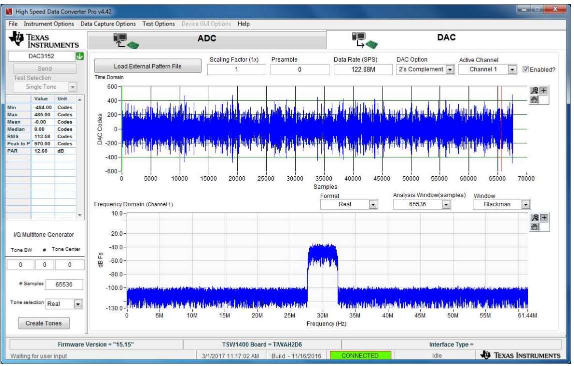
Figure: TI GUI Top level DAC Power
Analog Devices
EVAL-AD7380FMCZ/EVAL-AD7381FMCZ User Guide UG-1304
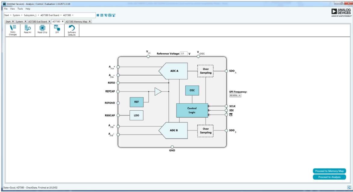
Figure: Analog Devices GUI DAC configuration
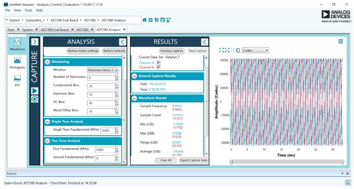
Figure: Analog Devices GUI Waveform
Waveform, histogram, FFT
Maxim, Renesenas
Summary
References
[1] P. Bourke. (1999, Dec.) "Interpolation Methods". Available: http://local.wasp.uwa.edu.au/~pbourke/
[2] Texas Instruments: ADC Evaluation Platform: PLABS-SAR-EVM-PDK, 499.-
[3] Renesas KMB001 Evaluation ADC System Mouser 351.-
[4] Digilent BASYS3 XADC Demo, https://digilent.com/reference/programmable-logic/basys-3/demos/xadc
Local References
- Research summary
- EE Bench
- Charge pump
- Video EEbench
- 16 Bit R2R DAC Simulation Characterization
- FFT Implementation
- Trigger Implementation
- NEEBench

| Dr. Ing. Joerg E. Vollrath received 1989 his Dipl. Ing. and 1994 his Ph. D. in electrical engineering, semiconductor technology at the University of Darmstadt, Germany. Since then he worked for the memory division of Siemens and Infineon Technologies and Qimonda in various locations in the USA and Germany. He is now a Professor for Electronics at the University of Applied Science, Kempten, Germany. His expertise and interest lies in the field of design of analog and digital circuits, programmable logic, test, characterization, yield, manufacturing and reliability. He has published 30 papers and has currently 32 patents. |